Korean chipmakers
Samsung Elec to provide HBM3, packaging service to Nvidia
Samsung may thus ink a deal to manufacture Nvidia’s GPUs while attracting other Big Tech names with its packaging turnkey service
By Aug 01, 2023 (Gmt+09:00)
5
Min read
Most Read
LG Chem to sell water filter business to Glenwood PE for $692 million


KT&G eyes overseas M&A after rejecting activist fund's offer
Kyobo Life poised to buy Japan’s SBI Group-owned savings bank
StockX in merger talks with Naver’s online reseller Kream
Meritz backs half of ex-manager’s $210 mn hedge fund


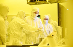
Samsung Electronics Co., the world’s top memory chipmaker, is set to provide high-performance semiconductors and packaging service to the global chip designer Nvidia Corp. for its graphics processing units, adding to expectations that the South Korean tech giant is likely to win orders from other Big Tech companies.
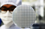
Samsung and Nvidia are working on technical verification for fourth-generation High Bandwidth Memory3 (HBM3) chips and packaging service for the US company’s GPUs, according to industry sources in Seoul on Tuesday.
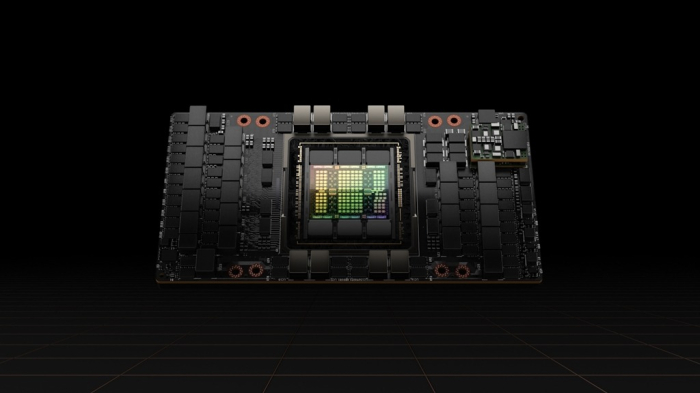
Once the work is completed, Samsung is expected to handle the packaging of H100, Nvidia’s latest artificial intelligence GPU, while supplying HBM3 chips for the processor. The two companies were known to sign a deal for the service and supply around year-end.
Packaging, one of the final steps in semiconductor manufacturing, places chips in a protective case to prevent corrosion and provides an interface to combine and connect already-made chips.
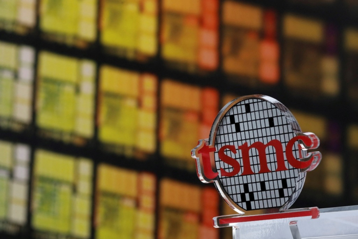
Nvidia has been heavily relying on Taiwan Semiconductor Manufacturing Co. (TSMC), which packages GPUs produced with its own foundry process, and SK Hynix Inc.'s HBM3 to manufacture the US company’s GPUs.
Nvidia started working with Samsung, however, as the US tech behemoth has been looking for other package service providers with TSMC’s process lines fully occupied amid surging demand for AI semiconductors. Samsung with semiconductor packaging capabilities plans to mass-produce HBM3 chips for GPUs.
The cooperation raised hopes that Samsung may ink a deal to manufacture Nvidia’s GPUs.
“More Big Tech names are predicted to look to Samsung as TSMC’s packaging process lines are booked up,” said an industry source in Seoul.
ADVANCED PACKAGING
Global semiconductor majors including Samsung, TSMC and Intel Corp. are fiercely competing for advanced packaging, the state-of-art technology that integrates different semiconductors or vertically interconnects multiple chips. Advanced packaging allows multiple devices to be merged and packaged as a single electronic device.
The global advanced packaging market was forecast to surge by 74% to $65 billion by 2027 from $37.4 billion in 2021, according to industry consulting firm Yole Intelligence.
The technology has been rapidly increasing in line with growth in generative AI such as ChatGPT, a chatbot developed by Microsoft Corp.-backed OpenAI, which requires semiconductors with the processing capacity of large data.
The global semiconductor industry is struggling to improve chip performance with ultra-fine processes. But the costs to develop new technology ballooned as the industry started producing chips with node sizes 3 nanometers or smaller.
Chipmakers and their customers paid attention to advanced packaging technologies that increase performance through efficient arrangement of existing semiconductors.
The industry is currently focusing on 2.5D packaging, which places GPUs and HBM chips, which are 10 times faster than the existing DRAM, as close together as possible to reduce data bottleneck.
TSMC, the world’s top foundry player, is currently leading the global advanced packaging market as it has been developing 2.5D packaging technology for a decade. The company last month said it plans to invest 90 billion Taiwanese dollars ($2.9 billion) in a new domestic advanced packaging plant.
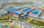
Samsung, the world’s No. 2 foundry company, is also accelerating the development of advanced packaging technology.
The company unveiled its own 2.5D packaging technology I-Cube in 2021. It is known to plan to mass-produce I-Cube4, which places four HBM chips with a GPU, from the second quarter of 2024 and I-Cube8, which uses eight HBM chips, from the third quarter of next year.
FOUNDRY PACKAGING TURNKEY SERVICE
Samsung aims to attract global major technology companies with its packaging turnkey service for contract chip manufacturing.
Samsung earlier this year launched the service, which covers the entire semiconductor manufacturing process including memory chip supplies, packages and tests as it aims to take on TSMC amid rapid growth in the AI industry.
The South Korean company provides one-stop services for the whole production by producing fabless system chips and packaging them with its own DRAM.
Demand for such a turnkey service is expected to grow as customers are likely to save time and costs by working with a foundry that has DRAM production and packaging capabilities, rather than using multiple contractors for each service.
“Semiconductor companies have a lot of trouble finding foundry, DRAM and packaging companies one by one,” said another industry source in Seoul. “Samsung’s turnkey service is expected to have a significant impact on the industry."
MORE DEALS FOR FOUNDRY, HBM
Samsung aims to bag more orders for contract chip manufacturing and HBM supplies through the package turnkey service.
At a June forum the company already predicted the service would increase foundry customers.
That is likely to improve its competitiveness in the HBM market where it is up against rivals such as SK Hynix and Micron Technology Inc. as Samsung will use its own products for the service.
The company launched the Multi-Die Integration Alliance in June to advance packaging technology with memory chip companies, outsourced semiconductor assembly and test firms and chip design houses.
Samsung’s rivals, however, played down the strategy.
“Customers do not want one company like Samsung to handle both memory and system semiconductor processes,” said an official of its competitor, indicating that semiconductor companies might be wary of an extremely powerful contractor that handles the entire production.
(Updated with advanced packaging)
Write to Ik-Hwan Kim and Jeong-Soo Hwang at lovepen@hankyung.com
Jongwoo Cheon edited this article.
More to Read
-
 Korean chipmakersSamsung improves 4 nm foundry yields, on par with TSMC: analyst
Jul 11, 2023 (Gmt+09:00)
4 Min read -
 Korean chipmakersSamsung, SK Hynix in next-generation HBM chip supremacy war
Jul 10, 2023 (Gmt+09:00)
3 Min read -
 Korean chipmakersSamsung Electronics to aid foundry clients with state-of-the-art tech
Jul 05, 2023 (Gmt+09:00)
3 Min read -
 Korean chipmakersSamsung on smooth track to 1.4 nm foundry tech to take on TSMC
Jun 28, 2023 (Gmt+09:00)
4 Min read -
 Korean chipmakersSamsung foundry backlogs top $74.6 bn for logic chip biz goal
Apr 30, 2023 (Gmt+09:00)
3 Min read -
 Korean chipmakersSamsung Elec launches foundry package turnkey service
Apr 14, 2023 (Gmt+09:00)
3 Min read -
 Korean chipmakersTSMC-Nvidia alliance step up 2 nm chip rivalry with Samsung
Mar 29, 2023 (Gmt+09:00)
2 Min read -
 Korean chipmakersSamsung Foundry: Driving force behind digital transformation
Dec 01, 2022 (Gmt+09:00)
5 Min read
Comment 0
LOG IN