Korean chipmakers
TSMC-Nvidia alliance step up 2 nm chip rivalry with Samsung
The move comes as both TSMC and Samsung aim to produce 2 nm chips by 2025
By Mar 29, 2023 (Gmt+09:00)
2
Min read
Most Read
LG Chem to sell water filter business to Glenwood PE for $692 million


KT&G eyes overseas M&A after rejecting activist fund's offer
Kyobo Life poised to buy Japan’s SBI Group-owned savings bank
StockX in merger talks with Naver’s online reseller Kream
Meritz backs half of ex-manager’s $210 mn hedge fund


TSMC Co. appears to be at the forefront of efforts to produce ultra-advanced semiconductor chips as the world's largest contract chip manufacturer is tightening its collaboration with Nvidia Corp., a US chip designer, to produce the industry's smallest 2-nanometer chips.
Taiwan-based TSMC has decided to apply Nvidia’s recently released lithography technology “cuLitho” to its fabrication process from June, according to semiconductor industry sources on Tuesday.
The US fabless company said the software system would accelerate the manufacturing and computational lithography process for semiconductors.
Its tie-up with TSMC comes as the Taiwanese foundry leader is gearing up to produce 2 nm chips by 2025, by when Samsung also aims to commercialize 2 nm process technology.
Currently, the 3 nm node is the most advanced semiconductor technology, for which Samsung and TSMC have been competing to improve production yields.
Smaller chips, or those with reduced circuit linewidth, are being used for high-performance products such as artificial intelligence and autonomous driving systems. But a smaller process node causes leakage currently because of the difficulty in the control of electric current flows.
Lithography is used to project transformational patterns on the photomask onto the surface of the wafer.
Nvidia said the cuLitho lithography technology is based on a graphic processing unit and would cut power consumption by 85%, compared with conventional technology based on a central processing unit.
An Nvidia official in Seoul said the cuLitho software will enable 2 nm contract chip manufacturers to reduce the lithography time, as well as improve its process accuracy.
Earlier this month, Intel Corp. said it had developed technologies to produce both 2 nm and 1.8 nm chips, one year ahead of schedule.
The announcement comes after it jumped into the foundry business to produce chips in-house and to reduce its dependence on chipmakers.
Last year, TSMC announced a plan to begin 2 nm chip production by 2025, according to a Nikkei report.
To that end, it is building a new plant in Taiwan to manufacture 2 nm chips, as part of its roadmap to spend a total of 100 trillion won ($770 million) to construct four plants.
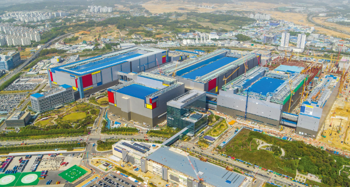
To narrow its gap with TSMC, Samsung is building three new semiconductor factories in its Pyeongtaek production complex near Seoul, which industry watchers said would have the 2 nm production infrastructure.
Up to now, Samsung has been seen to be ahead of TSMC in terms of technology to produce ultra-small chips. Last year, it became the world’s first memory chipmaker to mass produce 3 nm chips and then significantly improved its production yields.
The South Korean tech giant plans to apply its proprietary gate-all-around (GAA) transistor architecture to mass produce 2 nm chips. The GAA architecture was already adopted into its 2 nm process node.
The GAA architecture is a next-generation foundry microfabrication process. It is a key technology to improve electrostatic properties that translate into increased performance, reduced power and optimal chip designs, according to Samsung.
Samsung Electronics took a 15.8% share in the world’s foundry market as of end-2022, far behind TSMC’s 58.5%, according to TrendForce, a data provider.
Write to Jeong-Soo Hwang at hjs@hankyung.com
Yeonhee Kim edited this article
More to Read
-
 Korean chipmakersSamsung's foundry sales nearly match DRAM revenue
Mar 20, 2023 (Gmt+09:00)
2 Min read -
 Korean chipmakersSamsung’s 3 nm chip production yield rises sharply
Jan 09, 2023 (Gmt+09:00)
2 Min read -
 Korean chipmakersSamsung to make 3 nm chips for Nvidia, Qualcomm, IBM, Baidu
Nov 22, 2022 (Gmt+09:00)
3 Min read -
 Korean chipmakersSamsung's 3 nm chip narrows microchip gap with TSMC
Jun 30, 2022 (Gmt+09:00)
3 Min read -
 Korean chipmakersSamsung surprises foundry industry with plan for 2 nm chips
Oct 10, 2021 (Gmt+09:00)
3 Min read -
 Korean chipmakersSamsung to make 2-nanometer GAA chips by 2025 to overtake TSMC
Oct 07, 2021 (Gmt+09:00)
3 Min read -
 Korean chipmakersSamsung, TSMC in heated race for industry’s smallest 3 nm process node
Aug 04, 2021 (Gmt+09:00)
4 Min read
Comment 0
LOG IN