Korean chipmakers
Samsung’s 3 nm chip production yield rises sharply
Samsung is believed to reach a "perfect-level" production yield for the chips based on the world's smallest process node
By Jan 09, 2023 (Gmt+09:00)
2
Min read
Most Read
LG Chem to sell water filter business to Glenwood PE for $692 million


KT&G eyes overseas M&A after rejecting activist fund's offer
Kyobo Life poised to buy Japan’s SBI Group-owned savings bank
StockX in merger talks with Naver’s online reseller Kream
Meritz backs half of ex-manager’s $210 mn hedge fund


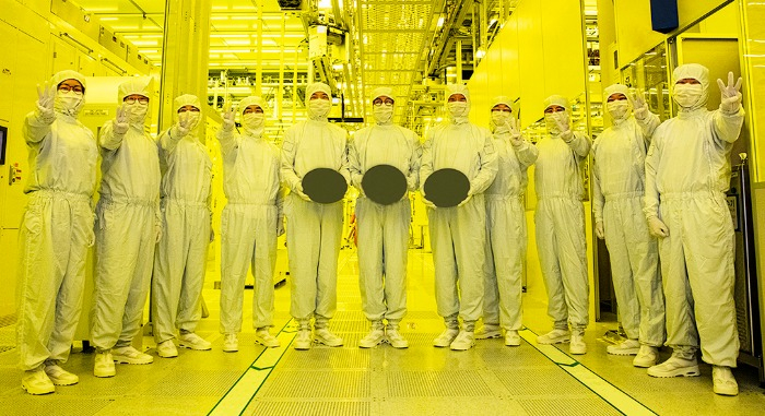
Samsung Electronics Co. has sharply increased its production yield of the industry’s most advanced 3-nanometer chips for fabless clients, according to industry sources on Monday, just as foundry leader TSMC Co. started mass production of the smallest chips.
Last year, the world’s largest memory chipmaker kicked off mass production of 3 nm chips as a global first. They were delivered to a Chinese fabless company.
At the time, the production yield of Samsung’s 3 nm chips was speculated to remain in the 10% range.
Now Samsung’s first-generation 3 nm process node reached “a perfect level” of production yields, said a source with knowledge of the situation, without elaborating further.
“We are now developing second-generation 3nm chips without delay,” he told The Korea Economic Daily.
Production yields means how many chips remain on the wafer and thus is the key to the profitability of the semiconductor process node.
The 3 nm technology is the first process node on which Samsung applied its s first-generation gate-all-around (GAA) structure transistors.
In a GAA transistor, the gate surrounds all four faces of the channel where electric current flows, thereby increasing a chip’s performance and energy efficiency.
By comparison, in the existing Fin field-effect transistor (FinFET) structure, the gate surrounds the channel from three sides.
Taiwan Semiconductor Manufacturing (TSMC) Co. sticks with the FinFET technology for 3 nm chips, which it started mass production late last month.
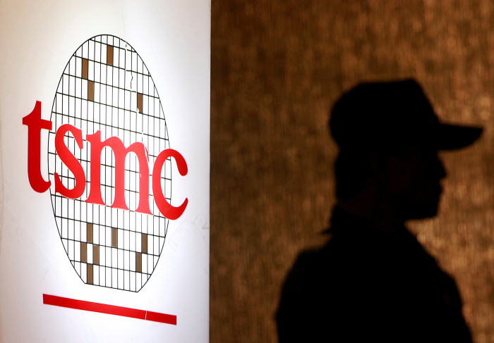
TSMC was about six months behind Samsung in mass producing the 3 nm chips. Apple Inc. is understood to be TSMC’s first customer for the most advanced chips.
Taiwanese media reported TSMC’s 3 nm process achieved a production yield of up to 85%, higher than Samsung’s.
But South Korean industry sources downplayed the report, saying the figure appeared to be exaggerated.
Considering TSMC’s mass production and delivery schedule of the industry's smallest chips to Apple, its production yield would be 50% at most, they said.
In November of last year, TSMC said its new factory in the US state of Arizona will have a 3 nm facility as well as 5 nm lines.
Now that TSMC adopts the 3 nm process node, industry observers said that 3 nm chips will likely become the mainstream product in the foundry market for the next couple of years.
The smaller process node, or reducing the circuit linewidth, causes current leakage because of difficulty in the control of electric current flows.
The 3 nm process node market is predicted to reach $25.5 billion by 2025, outstripping the estimated $19.3 billion for the 5 nm process
Samsung has been making semiconductors with the 3-nanometer technology for clients such as Nvidia, Qualcomm Technologies, Google and IBM and China’s Baidu, people familiar with the matter said in November.
Samsung Electronics takes a 16.4% share in the world’s foundry market as of end-September 2022, far behind TSMC’s 53.4%, according to TrendForce, a data provider.
Write to Jeong-Soo Hwang at hjs@hankyung.com
Yeonhee Kim edited this article
More to Read
-
 Korean chipmakersSamsung to make 3 nm chips for Nvidia, Qualcomm, IBM, Baidu
Nov 22, 2022 (Gmt+09:00)
3 Min read -
 Korean chipmakersSamsung's 3 nm chip narrows microchip gap with TSMC
Jun 30, 2022 (Gmt+09:00)
3 Min read -
 Korean chipmakersSamsung, TSMC in heated race for industry’s smallest 3 nm process node
Aug 04, 2021 (Gmt+09:00)
4 Min read
Comment 0
LOG IN