Korean chipmakers
Samsung's 3 nm chip narrows microchip gap with TSMC
Samsung starts mass production of the world's smallest chip as a global first and ahead of sector leader TSMC
By Jun 30, 2022 (Gmt+09:00)
3
Min read
Most Read
LG Chem to sell water filter business to Glenwood PE for $692 million


KT&G eyes overseas M&A after rejecting activist fund's offer
Kyobo Life poised to buy Japan’s SBI Group-owned savings bank
StockX in merger talks with Naver’s online reseller Kream
Meritz backs half of ex-manager’s $210 mn hedge fund


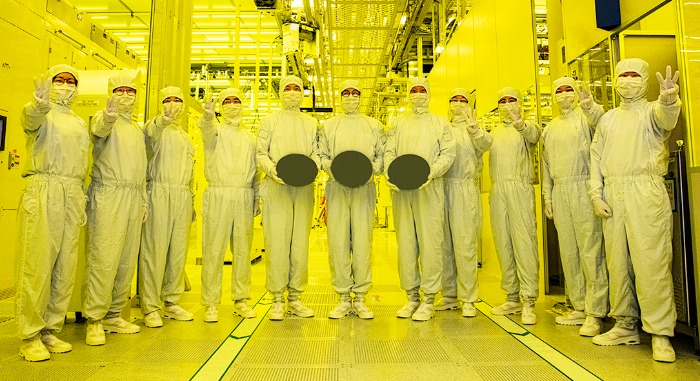
Samsung Electronics Co. has kicked off mass production of 3-nanometer chips based on the industry’s smallest process node as a global first, a move expected to narrow its gap with TSMC Co. in the advanced chip market.
The latest chip model employs Samsung’s first-generation gate-all-around (GAA) transistor technology, which increases a chip's performance and energy efficiency, the South Korean company said on Thursday.
The next-generation ultramicro fabrication process is expected to give the world’s top memory chipmaker an edge over foundry leader TSMC, which is understood to be preparing for volume production of 3 nm chips.
It remains uncertain when the Taiwanese company will start volume production for the smallest chip. Until now, 4 nm chips were the industry’s smallest for mass production.
TSMC controlled about half of the world’s foundry market last year, or three times that of Samsung’s 16.3%, according to research firm Omdia. Their market gap further widened in the first quarter of this year.
But in the microchip chip segment based on the 10 nm process node or below, the two companies have a smaller gap, splitting the market in a ratio of 6:4, with TSMC in a narrower lead.
“Currently, microchips are in demand mainly for servers and some mobile gadgets. But it will expand its range of application to other products,” said an industry insider.
“The bigger the microchip market, the narrower the gap will become between Samsung and TSMC.”

The foundry market for chips based on the 3 nm process node or below is forecast to grow by an average 85% per year through 2025, according to research firm Omdia. It is predicted to overtake both the 5 nm and 7 nm chips from 2024 in terms of sales.
In 2024, sales of 3 nm chips or smaller are predicted to reach $18.6 billion, bigger than $18.2 billion and $15.4 billion for 5 nm and 7 nm chips, Omdia forecasts. The gap is expected to grow bigger in the following years.
But production yields, which refer to how many chips remain on the wafer, will be the key to the profitability of the 3 nm process node.
“It usually takes three to four years to reach stable production yields,” said Yoo Hoi-jun, an electrical engineering professor at KAIST.
“To expand its presence, Samsung needs to shorten the time taken to reach that level.”
TECHNOLOGICAL CHALLENGES
Nano refers to the width of the chip circuit line. The thinner the circuit linewidth, the larger the number of chips can be mounted on a substrate or wafer.
However, reduction in the circuit linewidth causes current leakage because of difficulty in the control of electric current flows. That is why chipmakers have depended on the Fin field-effect transistor (FinFET) technology for 5 nm chips.
Due to such technological challenges, it has taken even more time than before for foundry players to develop a smaller process node, or further reduce the circuit linewidth.
The GAA technology sets it apart from the FinFet process since it allows for more delicate control of electric current flows within a chip than other chip models, thereby avoiding the performance degradation of microchips.
Moreover, the GAA process minimizes the size of a chip by 16%, while providing 23% higher performance or 45% lower power consumption, compared with the 5 nm process.
Samsung’s second-generation GAA process, set to be unveiled next year, will further reduce power consumption by 50%, improve performance by 30% and minimize the size by 35% in comparison to the 5 nm node.
Samsung will apply the 3 nm process to the production lines of system-on-a-chip for use in high-performance computers before expanding its adoption to mobile chips.
Further, Samsung plans to commercialize an advanced 2 nm GAA technology by 2025 with a goal of becoming the top player in the foundry market by 2030.
Until early this year, TSMC was expected to become the world’s first foundry company to develop the industry’s smallest process node.
Last August, the company began installing equipment for the next-generation 3 nm chip process node at its Fab 18 in Taiwan to prepare for mass production of chips in the second half of this year. Fab 18 is responsible for producing 5 nm chips.
Write to Shin-Young Park and Ji-Eun Jeong at nyusos@hankyung.com
Yeonhee Kim edited this article.
More to Read
-
 Korean chipmakersSamsung nears 3-nano chip mass production ahead of TSMC
Jun 28, 2022 (Gmt+09:00)
3 Min read -
 Korean chipmakersSamsung to make 2-nanometer GAA chips by 2025 to overtake TSMC
Oct 07, 2021 (Gmt+09:00)
3 Min read -
 Korean chipmakersSamsung, TSMC in heated race for industry’s smallest 3 nm process node
Aug 04, 2021 (Gmt+09:00)
4 Min read
Comment 0
LOG IN