Samsung nears 3-nano chip mass production ahead of TSMC
The chipmaker is expected this week to announce the microchip mass production based on a next-generation fabrication process
By Jun 28, 2022 (Gmt+09:00)
LG Chem to sell water filter business to Glenwood PE for $692 million


KT&G eyes overseas M&A after rejecting activist fund's offer
Kyobo Life poised to buy Japan’s SBI Group-owned savings bank
StockX in merger talks with Naver’s online reseller Kream
Meritz backs half of ex-manager’s $210 mn hedge fund


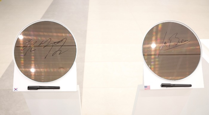
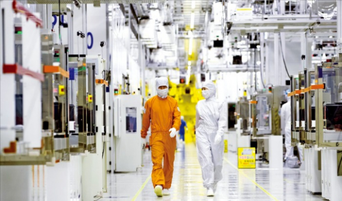
Samsung Electronics Co. is close to mass producing 3-nanometer chips based on a next-generation ultramicro fabrication process as a global first and ahead of Taiwan’s TSMC Co., according to industry sources on Tuesday.
The world’s top memory chipmaker is slated to announce mass production of the latest chip model based on its gate-all-around (GAA) transistor technology this week. The South Korean company is also considering whether or not to disclose its clients for the microchip.
“Samsung has been developing the GAA-based 3-nano chip without interruption,” one of the sources told The Korea Economic Daily.
“We will hear about its mass production this week.”
Samsung planned to broadly apply its first-generation GAA process technology to the volume production of foundry chips in the first half of this year. TSMC, the world's largest foundry company, is understood to be launching a 3 nm chip process this year.
Nano refers to the width of the chip circuit line. The thinner the circuit linewidth, the higher the chip performance and energy efficiency since a larger number of chips can be mounted on a substrate or wafer.
The upcoming chip will likely help Samsung expand its footprint in the foundry market, winning over Qualcomm Inc. and Nvidia Corp. as clients. It also expects to widen the gap with Intel Corp., which announced its re-entry into the foundry business last year.
GAA technology is key in increasing the performance and reducing the energy consumption of a chip since it allows for delicate control of electric current flows within a chip.
Morever, the GAA process minimizes the size of a chip by up to 35%, while providing about 30% higher performance or 50% lower power consumption, compared with the 5 nm process.
Until now, chipmakers have depended on the Fin field-effect transistor (FinFET) process. The GAA process is compatible with the FinFET process, thereby chipmakers will be able to shift into the new fabrication process without needing to change their production lines and equipment.
PRODUCTION YIELD
Mass production of the 3-nano chip is expected to quell market concerns about its production yield, which refers to how many chips remain on the wafer.
Last year, Samsung said it will be able to commercialize an advanced 2 nm GAA technology by 2025 with a goal of becoming the top player in the foundry market by 2030.
But it saw its market share declining and widening the gap with TSMC in the first three months of this year.
Samsung made up 16.3% of the foundry market as of the end of the first quarter, down from 18.3% three months earlier, according to research firm TrendForce. By contrast, TSMC increased its market share to 53.6% from 52.1% in the corresponding period.
Early this month, Samsung let go of several executives, including the flash chip development chief and the foundry business head. They were held accountable for the lower-than-expected yield of its new mobile application processor.
Following the unexpected personnel reshuffle, Samsung Electronics' de facto leader Jay Y. Lee visited the Netherlands-based ASML Holding NV, the world’s sole producer of extreme ultraviolet light (EUV) scanners, earlier this month. The EUV lithography machine is key in producing advanced chips.
Upon his return to Seoul last week, Lee picked his tour of the Dutch company as the most meaningful during his business trip to Europe, without elaborating further.
Last month, Samsung Group unveiled a 450 trillion won ($355 billion) investment plan for the next five years, for which Lee said it will take on with a do-or-die attitude.
Write to Kyung-Joo Kang at qurasoha@hankyung.com
Yeonhee Kim edited this article.
-
 Korean chipmakersSamsung holds emergency CEO meeting on technology, risk
Jun 20, 2022 (Gmt+09:00)
4 Min read -
 Corporate investmentSamsung to invest $355 billion in chip, biotech, 6G over five years
May 24, 2022 (Gmt+09:00)
3 Min read