As the contract chip manufacturing, or foundry, business is quickly emerging as the next battlefield for the world’s major chipmakers, The Korea Economic Daily is running a series of articles on Samsung Electronics, the world’s second-largest foundry player.
This is the third article in a three-part series on Samsung’s quest for global leadership. Read Part 1 and Part 2.
Samsung Electronics' foundry business chief Dr. Siyoung Choi There’s no denying that the modern history of technology is the history of semiconductors.
Microchips, often referred to as the brains of modern electronics, have never been more important than in the era of the Fourth Industrial Revolution. Chips are an integral part of almost everything called smart gadgets or smart services, including artificial intelligence, big data and the Internet of Things.
With exponential growth in demand for sophisticated and user-specific semiconductors, foundry, or chip manufacturing for chip designers and fabless companies, has for years been one of the industry’s toughest battlegrounds.
According to market research firm Omdia, the global foundry market is forecast to grow at an annual average rate of 13.4% to $145.6 billion by 2025 from an estimated $98.6 billion this year.
Global Foundry Market
Unit: billion dollars
Source: Omdia
Graphics by Jerry Lee
In the foundry market, staying ahead of rivals is challenging since it requires aggressive investments to expand facilities and continuous technological advancement to secure new clients.
Samsung Electronics Co., the world’s second-largest foundry player, is no stranger to this kind of challenge.
Samsung announced its Vision 2030 in April 2019, under which the company stressed the importance of its foundry business as one of the conglomerate's key growth drivers.
The company announced a 133 trillion won investment in R&D and production facilities for its Foundry and System LSI businesses through 2030.
In May 2021, the company unveiled further commitment by announcing a total investment of 171 trillion won, adding 38 trillion won to its previous commitment.
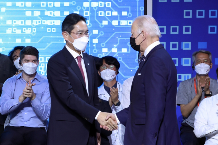
Samsung Group leader Jay Y. Lee shakes hands with US President Joe Biden at the chipmaker's Pyeongtaek plant during Biden's Korea visit in May 2022 TO TRIPLE CHIP OUTPUT CAPACITY BY 2027
While unveiling its advanced chip processing tech roadmap ahead of its archrival, Taiwan Semiconductor Manufacturing Co., the South Korean tech giant said at the Samsung Foundry Forum 2022, held in San Jose, California in October, that it aims to more than triple its advanced chip production capacity by 2027 compared to this year.
At a media briefing following the annual event, Moonsoo Kang, executive vice president and head of foundry business development at Samsung Electronics, said the number of the company’s foundry clients as of 2021 more than doubled from two years earlier.
Samsung’s foundry clients will rise fivefold by 2027 compared to 2019, he said.
As part of its efforts to achieve that goal, the company said it will also ensure non-mobile applications such as high-performance computing (HPC), 5G connectivity and automotive chips account for more than half of its foundry sales by then to diversify its business portfolio.
AUTOMOTIVE CUSTOMERS
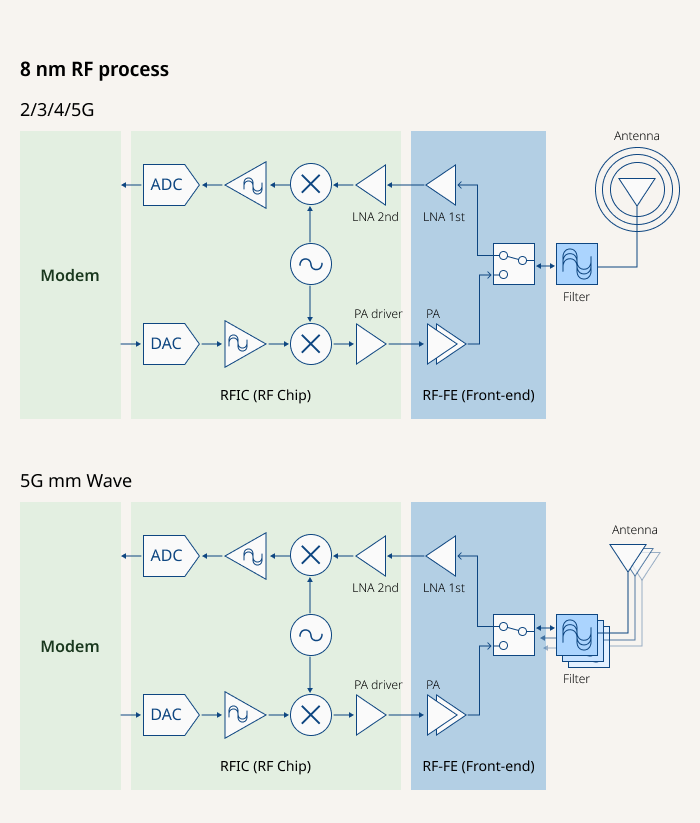
For automotive customers specifically, Samsung is providing embedded non-volatile memory (eNVM) solutions based on its 28-nanometer technology. To support automotive-grade reliability, the company plans to further expand process nodes by launching 14 nm eNVM solutions in 2024 and adding an 8 nm eNVM further down the road.
Samsung, which is already producing radio frequency (RF) products with a 14 nm process in large quantities, recently succeeded in the mass production of 8 nm RF products. The development of a 5 nm RF process is currently underway.
While pioneering process technologies, Samsung is also accelerating the development of 2.5D and 3D heterogeneous integration packaging technology to provide a total foundry services system solution.
Through continuous innovation, its 3D packaging X-Cube with micro-bump interconnection will be ready for mass production in 2024, and the bump-less X-Cube will be available by 2026.
Samsung Semiconductor Revenue
Unit: trillion won
Source: Samsung Electronics
Graphics by Jerry Lee
INTELLECTUAL PROPERTY PARTNERS
Samsung is also expanding partnerships with its clients for chip design intellectual properties (IPs), key assets for foundry players.
As of 2022, the company provides more than 4,000 IPs with 56 partners. It also cooperates with nine and 22 partners in the design solution and exploratory data analysis (EDA) business, respectively.
Samsung works with nine partners for cloud services and 10 partners for packaging services.
Through its IP partner program, called the Samsung Advanced Foundry Ecosystem (SAFE), the tech giant plans to identify new fabless customers by strengthening customized services with improved performance, rapid delivery and price competitiveness, while actively attracting new customers such as startups and hyperscalers or big enterprises that operate large-scale data centers.
Samsung’s Major Foundry Business Plan
Year
Plan
2024
Mass production of micro-bump X-Cube
Development of 14 nm automotive eNVM solution
2025
Introduction of 2 nm GAA tech
2027
Introduction of 1.4 nm GAA tech
Triple chip production capacity with Shell-First strategy
Samsung, which in June kicked off mass production of advanced chips based on its proprietary gate-all-around (GAA) technology, the industry’s smallest 3 nm process node, said in October it will start manufacturing chips on the 2 nm node in 2025 and move on to a more advanced 1.4 nm process in 2027.
“Our chip order balance for the next five years is eight times the sales figures for 2021,” said a Samsung Electronics official.
“With our advanced chip processing nodes, we expect more orders down the road.”
Write to Haeyoung Park at bono@hankyung.com In-Soo Nam edited this article.
We use cookies to provide the best user experience. By continuing to browse this website, you will be considered to accept cookies. Please review our Privacy Policy to learn our cookie policy.


 Korean chipmakersShell-First: Samsung Foundry’s custom-tailored new operation strategy
 Korean chipmakersSamsung sets sights on GAA tech to overtake TSMC in foundry
 Korean chipmakersSamsung Elec to expand foundry business to tackle TSMC
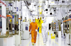 Korean chipmakersSamsung to ramp up hiring for foundry business