As the contract chip manufacturing, or foundry, business is quickly emerging as the next battlefield for the worldŌĆÖs major chipmakers, The Korea Economic Daily is running a series of articles on Samsung Electronics, the worldŌĆÖs second-largest foundry player.
This is the first article in a three-part series on SamsungŌĆÖs quest for global leadership.
Samsung's foundry head Dr. Siyoung Choi unveils a new tech roadmap at Samsung Foundry Forum 2022
The news was proof that the worldŌĆÖs top memory maker has improved its production yield to make its clients happy. During its third-quarter earnings call, Samsung announced record quarterly sales and net profit, which it attributed to its improved yield of advanced nodes.
The news also came amid market chatter that its archrival, Taiwan Semiconductor Manufacturing Co., could be behind schedule in the launch of its 3 nm tech for mass production.
The rivalry between the worldŌĆÖs two largest contract chipmakers has been intensifying with their key former client, namely, Intel Corp., also throwing down the gauntlet to reenter the fast-growing foundry business.
Samsung and TSMC are particularly keen to employ the 3 nm process node, the industryŌĆÖs narrowest circuitry, to manufacture chips with increased transistor density, faster data speed and reduced power consumption.
ŌĆ£The 3-nanometer technology is a game changer in the foundry industry,ŌĆØ Sang-Pil Sim, executive vice president and head of foundry marketing and sales at Samsung Electronics, said during a meeting with institutional investors at Samsung Electronics Investors Forum held on Nov. 15.
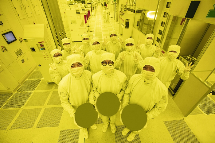
Samsung executives hold semiconductor wafers made with 3-nanometer tech FIRST MOVER VOWING TO ASCEND TO THE THRONE
With the demand for high-performance computing (HPC) chips used in supercomputers and computer clusters rising, competition for technology advancement is also fierce.
By multiple measures, TSMC and Samsung stand at the final stretches of their pursuit of miniaturizing chip circuitry and harnessing new production techniques.
In June, Samsung said it has┬Ākicked off┬Āmass production of advanced chips based on the industryŌĆÖs smallest process node┬Āas a global first.
Chipmaking processes carry a numerical label that loosely denotes the size of the transistors that can be packed on a chip. The number implies the thickness of the circuitry that can be drawn on the transistor. The lower the nanometer number, the more advanced the technology.
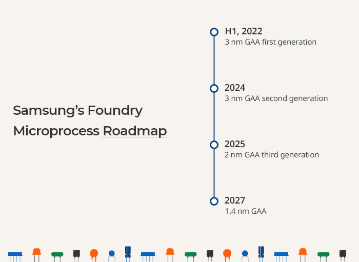
Samsung says its first generation 3 nm tech improves power efficiency and chip performance by 45% and 23%, respectively, compared with its earlier 5 nm node. The new tech also reduces chip surface area by 16%.
Further, Samsung said it plans┬Āto commercialize more advanced 2 nm technology by 2025┬Ā and 1.4 nm by 2027 to become┬Āthe top player in the non-memory market, including the foundry business, no later than 2030.
The company operates contract chipmaking facilities in Giheung, Hwaseong and Pyeongtaek in Korea; and Austin in the US state of Texas, with its Taylor fab set to begin manufacturing by 2024.
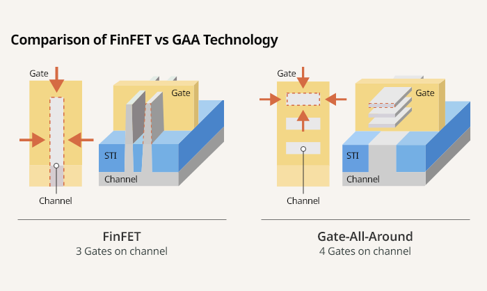
GAA VS FINFET
Samsung and TSMC, the two dominant foundry players, use different technologies for their 3 nm nodes.
SamsungŌĆÖs production tech is based on its proprietary gate-all-around (GAA) transistor architecture, a next-generation foundry microfabrication process.
Meanwhile, TSMC and other foundry companies use a technology called fin field-effect transistor (FinFET) process. Since its structure resembles a fishŌĆÖs dorsal fin, it is also called the fin transistor.
A transistor is composed of a channel in which the electric current flows between the semiconductorŌĆÖs source and its drain and a gate for managing the electric current traveling through the channel.
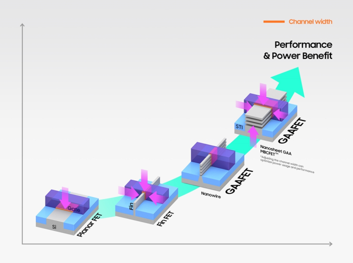
The evolution of semiconductor transistors┬Ā
While the chip industry increasingly requires transistors that can significantly reduce the operating voltage, the fin transistorŌĆÖs three-dimensional structure, where only three of the four channels are in contact with gates, has shown limitations in taking the chip technology to the next level.
To mitigate such limitations of existing transistors, Samsung developed a new architecture, GAA. As the name suggests, the GAA structure maximizes gatesŌĆÖ channel-controlling function, as all channels, including the fourth bottom one, are covered by gates.
SamsungŌĆÖs GAA technology, known as the multi-bridge-channel FET, or MBCFET, defies the performance limits of FinFET, improving power efficiency by reducing the supply voltage level while enhancing performance by increasing drive current capability, the company said.
ŌĆ£The development of GAA transistors is the Industrial Revolution in the chip sector. Our MBCFET has laid the foundation for transforming the chip industry that was set to stall at the 4-nanometer scale,ŌĆØ it said.
Dr. Siyoung Choi, president and head of the foundry business at Samsung Electronics, said: ŌĆ£Samsung has demonstrated its leadership in applying next-generation technologies to manufacturing, such as the foundry industryŌĆÖs first High-K Metal Gate, FinFET as well as EUV. We will continue our leadership with the worldŌĆÖs first 3-nanometer MBCFET process.ŌĆØ
Samsung said it is now applying the 3 nm GAA tech to its manufacturing process at the Hwaseong plant but plans to soon use the node for mass production at its main Pyeongtaek plant.
Graphics by Jerry Lee VISION 2030
In May 2021, Samsung announced SamsungŌĆÖs Vision 2030, under which the company stressed the importance of the foundry business as one of the conglomerate's key growth drivers.
The company announced an investment of 171 trillion won($129 billion) for R&D and production facility for its Foundry and System LSI businesses through 2030, adding 38 trillion won to its previous commitment of 133 trillion won announced in April 2019.
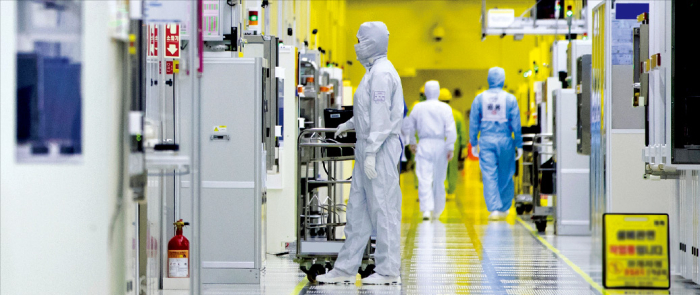
Samsung Electronics' chip clean room Industry watchers said Samsung is expanding its foundry business as the global market for system chips is growing rapidly in tandem with the takeoff of autonomous driving, artificial intelligence, robots and drones.
Samsung said its foundry business posted record sales revenue and operating profit for two straight quarters starting in the April-June period.
ŌĆ£On an annual basis, we expect the highest sales and profit from the foundry business in 2022,ŌĆØ said Moonsoo Kang, executive vice president and head of foundry business development at Samsung Electronics.
ŌĆ£WeŌĆÖll further advance our process technology to make a variety of products, including automotive chips and IoT chips, while trying to secure new clients.ŌĆØ
Write to Haeyoung Park at bono@hankyung.com In-Soo Nam edited this article.
We use cookies to provide the best user experience. By continuing to browse this website, you will be considered to accept cookies. Please review our┬ĀPrivacy Policy┬Āto learn our cookie policy.


 Korean chipmakersSamsung to make 3 nm chips for Nvidia, Qualcomm, IBM, Baidu
 Korean chipmakersSamsung mulls new foundry plant in Europe, to expand outsourcing
 The KED ViewCan Samsung Electronics ever catch up to foundry leader TSMC?
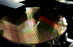 Korean chipmakersSamsung, TSMC in heated race for industryŌĆÖs smallest 3 nm process node
 Korean chipmakersMemory leader Samsung aims to strengthen system chips, foundry
Comment 0