Korean chipmakers
Samsung Elec launches foundry package turnkey service
Samsung focuses on technology of packaging DRAMs with CPUs to attract Big Tech names including Google as customers
By Apr 14, 2023 (Gmt+09:00)
3
Min read
Most Read
LG Chem to sell water filter business to Glenwood PE for $692 million


KT&G eyes overseas M&A after rejecting activist fund's offer
Kyobo Life poised to buy Japan’s SBI Group-owned savings bank
StockX in merger talks with Naver’s online reseller Kream
Meritz backs half of ex-manager’s $210 mn hedge fund


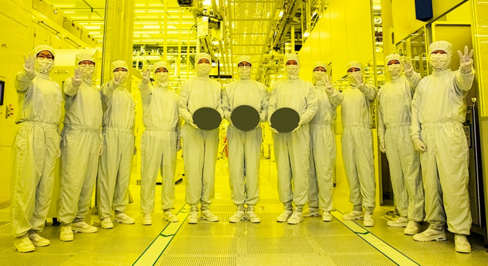
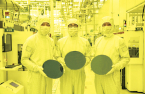
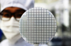
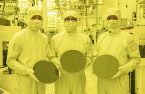
Samsung Electronics Co., the world’s No. 2 foundry player, has begun package turnkey service for contract chip manufacturing as it aims to take on global leader Taiwan Semiconductor Manufacturing Co. (TSMC) amid rapid growth in the artificial intelligence sector.
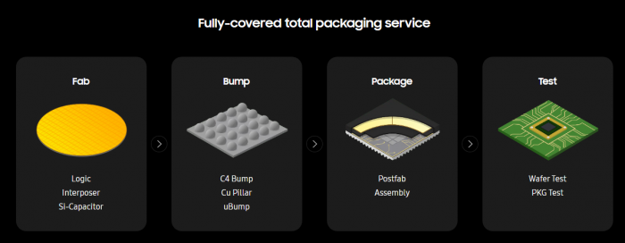
The South Korean tech giant’s foundry business division handles the entire whole chip packaging process from production to tests with the service, bringing precision to every step of the process and optimizing customers’ product cycles.
The world’s top memory chipmaker is focusing on the technology of packaging its flagship products such as DRAMs together with central processing units (CPUs) to attract Big Tech names such as Alphabet Inc.’s Google LLC, which are developing their own AI semiconductors, as customers for the service.
“Samsung is a comprehensive semiconductor maker, which can work on all businesses including fabless, memory chip production, foundry and packaging,” a company official said. “We provide the best performance at all stages of the chip manufacturing process to help customers’ innovation.”
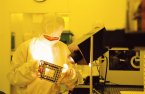
The company plans to provide advanced technologies such as 2.5D and 3D IC packaging. 2.5D and 3D are packaging methodologies for including multiple IC inside the same package. In a 2.5D structure, two or more active semiconductor chips are placed side-by-side on a silicon interposer for achieving extremely high die-to-die interconnect density. In a 3D structure, active chips are integrated by die stacking for the shortest interconnect and smallest package footprint.
Samsung is also set to cooperate with other companies such as Amcor plc, the world’s No. 2 back-end processing firm, to provide necessary services quickly, depending on customers’ situations.
GROWING MARKET
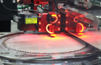
The move came as the global semiconductor industry is struggling to improve chip performance with ultra-fine processes. Chipmakers and their customers paid attention to advanced packaging technologies that increase performance through efficient arrangements of existing semiconductors.
The advanced packaging industry is rapidly growing. The global market was forecast to nearly triple to $7.9 billion by 2027 from $2.7 billion in 2021, according to a market research firm Yole Development SA.
Samsung already took various measures to expand its presence in the market. The company developed high bandwidth memory (HBM), which enables the process of large-sized data by combining multiple DRAMs while advancing heterogeneous integration technology that connects HBMs and CPUs.
Late last year, the company established a team for the advanced packaging business under the direct control of Kyung Kye Hyun, president and CEO of Samsung’s device solution division that handles global operations of the memory, system LSI and foundry business units.
BIG TECH CUSTOMERS
Samsung aims to lure Big Tech names such as Google, Microsoft Corp., Tencent Holdings and others, which are improving their services by advancing AI and high-performance computing technologies, for the package turnkey service. Those global tech giants need high-performance semiconductors through advanced packaging for development.
Samsung’s packaging service allows those companies to shorten the time for semiconductor procurement and cut costs for supply chain management, the South Korean tech behemoth said.
“We are helping customers deal with the rapid change in market demand,” the Samsung official said.
The company also hopes to bite into the market share of the world’s top foundry player TSMC, which accounts for more than 50% of the global industry.
TSMC, which already operates five plants only for packaging in Taiwan, opened a research and development center for 3D IC packaging technologies in Ibaraki Prefecture, Japan, in June last year.
Write to Jeong-Soo Hwang at hjs@hankyung.com
Jongwoo Cheon edited this article.
More to Read
-
 Korean chipmakersSamsung's foundry sales nearly match DRAM revenue
Mar 20, 2023 (Gmt+09:00)
2 Min read -
 Korean chipmakersSystem on chips: Samsung’s new high-stakes foundry business
Mar 09, 2023 (Gmt+09:00)
2 Min read -
 Korean chipmakersSamsung may cut spending as foundry players brace for downturn
Jan 13, 2023 (Gmt+09:00)
3 Min read -
 Korean chipmakersSamsung’s foundry revenue exceeds mainstay NAND chip sales
Dec 13, 2022 (Gmt+09:00)
3 Min read -
 Korean chipmakersSamsung Foundry: Driving force behind digital transformation
Dec 01, 2022 (Gmt+09:00)
5 Min read -
 Korean chipmakersShell-First: Samsung Foundry’s custom-tailored new operation strategy
Nov 30, 2022 (Gmt+09:00)
4 Min read -
 Korean chipmakersSamsung sets sights on GAA tech to overtake TSMC in foundry
Nov 29, 2022 (Gmt+09:00)
6 Min read -
 Korean chipmakersSamsung Elec to expand foundry business to tackle TSMC
Oct 24, 2022 (Gmt+09:00)
3 Min read
Comment 0
LOG IN