Korean chipmakers
Samsung, SK Hynix in next-generation HBM chip supremacy war
SK is slated to hold a closed-door IR session Wednesday to show off its tech as competition with Samsung heats up
By Jul 10, 2023 (Gmt+09:00)
3
Min read
Most Read
LG Chem to sell water filter business to Glenwood PE for $692 million


KT&G eyes overseas M&A after rejecting activist fund's offer
Kyobo Life poised to buy Japan’s SBI Group-owned savings bank
StockX in merger talks with Naver’s online reseller Kream
Meritz backs half of ex-manager’s $210 mn hedge fund


Samsung Electronics Co. and SK Hynix Inc. – the world’s two largest memory chipmakers – have fiercely competed to advance their chip stacking technology to cut costs and improve performance.
With the takeoff of ChatGPT, a generative AI chatbot that responds to questions in humanlike ways, the two South Korean companies are now waging another tech war to meet growing demand for high-capacity, high-performance semiconductors, called High Bandwidth Memory (HBM).
This Wednesday, SK Hynix, the No. 2 memory player, will hold a closed-door investor relations session in Seoul to brief institutional investors, including the National Pension Service, and analysts on the chipmaker’s HBM capabilities, industry sources said on Monday.
Unlike typical IR sessions, which usually focus on earnings and business strategies, the upcoming IR meeting will be a technology seminar to show off SK’s tech prowess, sources said.
Two HBM chip experts together with IR executives will host the session, they said.
HBM, a type of DRAM, is used to power generative AI devices, high-performance data centers as well as machine learning platforms that enhance the functioning of artificial intelligence and super-computing performance.
In the HBM DRAM segment, SK Hynix has been leading the pack for years.
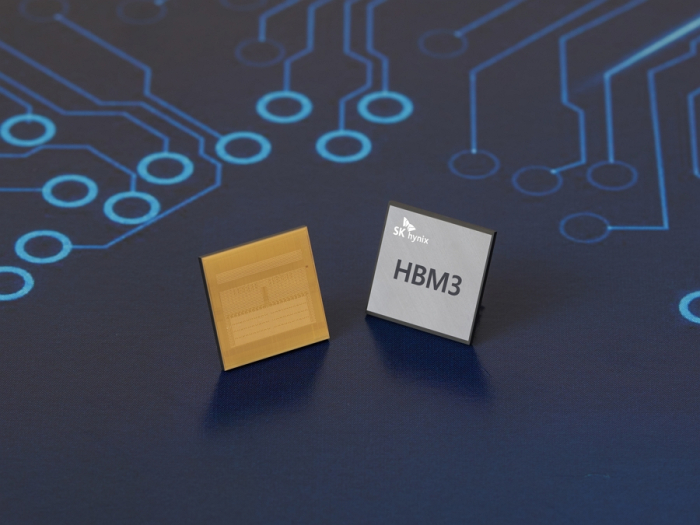
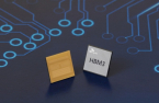
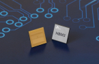
The company was the first memory vendor to develop the first-generation HBM chip in 2013 and unveiled succeeding products – HBM2, HBM2E and the latest and fourth-generation HBM3 chips in following years.
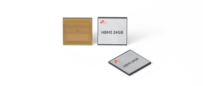
In April, SK said it has developed the world’s first 12-layer HBM3 DRAM product with a 24 gigabyte (GB) memory capacity, the industry’s largest and slimmest.
It has provided samples to its customers with an aim to begin mass production later this year.
SK said the 24 GB package product increases the memory capacity by 50% compared with earlier products. Existing HBM3 products’ maximum memory capacity was 16 GB and came with an 8-layer configuration.
The company’s latest 12-layer, 24 GB HBM3 boasts a data process speed of up to 819 GB per second, capable of transmitting 163 full-HD movies in a single second.

SAMSUNG FIGHTS BACK
Samsung also aims to begin mass production of HBM3 chips by year’s end.
Company officials said it will spend hundreds of billions of won to double its HBM3 chip manufacturing capacity at its Cheonan plant by the end of 2024.
Samsung will supply its products to fabless chip designer Advanced Micro Devices Inc. (AMD) and other clients, sources said.
According to local brokerage KB Securities, HBM3 will account for 18% of its chip sales revenue in 2024, up from an estimated 6% this year.
Kyung Kye-hyun, president and head of Samsung’s Device Solutions division, which oversees its chip business, said at a company meeting earlier this month that Samsung will strive to control more than half the HBM market.
“We’re receiving positive responses from our clients on our HBM3 products,” he said.
Samsung Chairman Jay Y. Lee, during his US trip in May met with Nvidia Chief Executive Jensen Huang to discuss ways to expand their business partnership, particularly in GPU and application process (AP) chips.
HBM CHIPS, KEY TO PROFITS
Both Samsung and SK Hynix hope their semiconductor businesses turn to profit with increased sales of high-capacity chips such as HBM.
HBM chips, which vertically interconnect multiple DRAM chips and dramatically increase data processing speed compared to traditional DRAM products, are at least five times more expensive than commodity DRAMs.
Analysts expect Samsung’s chip division and SK Hynix to post record first-half operating losses of 8.5 trillion won ($6.5 billion) and 6.3 trillion won, respectively, when they announce their results later this month.
In the second quarter alone, Samsung’s chip business likely posted nearly 4 trillion won in operating losses, analysts said.
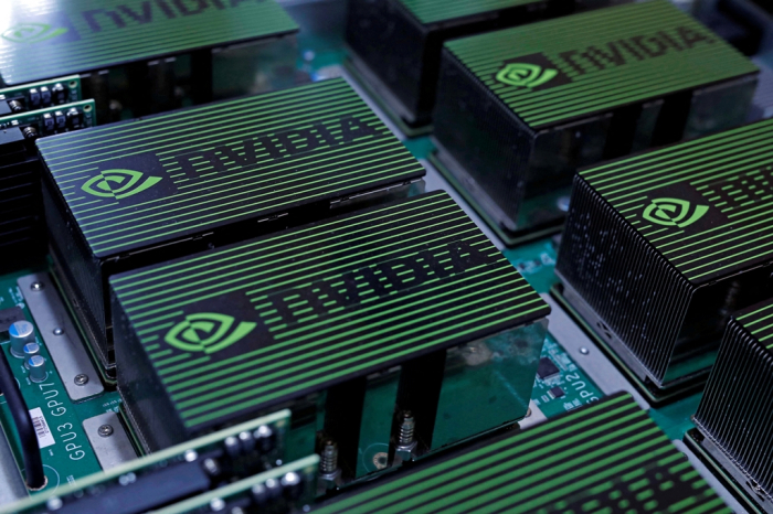
SK Hynix is already supplying its HBM3 DRAM chip to US graphic chipmaker Nvidia Corp. for its graphic processor unit H100.
AMD also said recently that it will adopt SK’s HBM3 to power its M1300X AI chips.
According to market tracker TrendForce, SK Hynix led the HBM market with a 50% market share as of 2022, followed by Samsung (40%) and Micron Technology Inc. (10%).
Global shipments of HBM chips are forecast to increase 58% this year from last year, according to TrendForce.
Write to Ik-Hwan Kim at lovepen@hankyung.com
In-Soo Nam edited this article.
More to Read
-
 EarningsSamsung chip turnaround likely in second half after dismal Q2
Jul 07, 2023 (Gmt+09:00)
3 Min read -
 Korean chipmakersSK Hynix steps up chip stacking war with 238-layer 4D NAND
Jun 08, 2023 (Gmt+09:00)
3 Min read -
 Samsung GroupSamsung's Lee to redefine growth roadmap with focus on new drivers
May 12, 2023 (Gmt+09:00)
3 Min read -
 Korean chipmakersSK Hynix unveils industry’s slimmest 12-layer, 24 GB HBM3 chip
Apr 20, 2023 (Gmt+09:00)
2 Min read -
 Korean chipmakersSK Hynix to supply industry’s best-performing DRAM to Nvidia
Jun 09, 2022 (Gmt+09:00)
1 Min read -
 Korean chipmakersSK Hynix unveils industry’s highest-performing DRAM chip
Oct 21, 2021 (Gmt+09:00)
2 Min read
Comment 0
LOG IN