Korean chipmakers
SK Hynix unveils industry’s slimmest 12-layer, 24 GB HBM3 chip
The company aims to consolidate its market leadership with the latest chip for AI, chatbot applications
By Apr 20, 2023 (Gmt+09:00)
2
Min read
Most Read
LG Chem to sell water filter business to Glenwood PE for $692 million


KT&G eyes overseas M&A after rejecting activist fund's offer
Kyobo Life poised to buy Japan’s SBI Group-owned savings bank
StockX in merger talks with Naver’s online reseller Kream
Meritz backs half of ex-manager’s $210 mn hedge fund


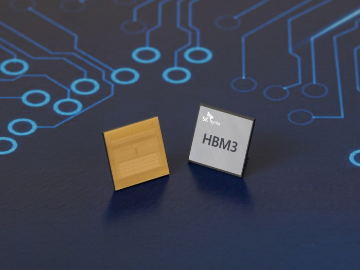
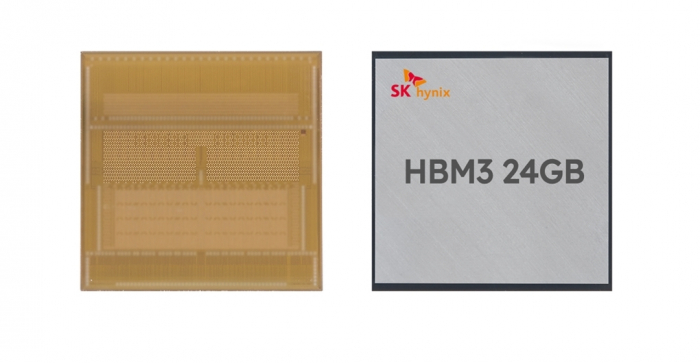
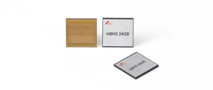
SK Hynix Inc., the world’s second-largest memory chipmaker, said on Thursday it has developed the world’s first 12-layer DRAM product with a 24 gigabyte (GB) memory capacity, the industry’s largest.
Called HBM3, short for High Bandwidth Memory 3, the chip is the fourth-generation DRAM memory, succeeding the previous generations – HBM, HBM2 and HBM2E – and is the slimmest of its kind.
The South Korean chipmaker said it has already provided samples to its customers and the chip's performance evaluation is currently underway.
The 24 GB package product increases the memory capacity by 50% compared with earlier products. Existing HBM3 products’ maximum memory capacity was 16 GB and came with an 8-layer configuration.
“We will be able to supply the new products to the market from the second half of the year, in line with growing demand for premium memory products driven by the AI-powered chatbot industry,” the company said.
SK Hynix was the first memory vendor to start mass production of the world’s first HBM3 in June 2022.
The company said at the time it will supply the HBM3 DRAM to US graphic chipmaker Nvidia Corp. for its graphic processor unit H100.
AI, CHATBOT APPLICATIONS
Industry watchers said HBM DRAM is in growing demand as the chip powers generative AI devices that operate on high-performance computing systems.
The company’s latest 12-layer, 24 GB HBM3 boasts a data process speed of up to 819 GB per second, capable of transmitting 163 full-HD movies in a single second.
To make the 12-layer chip, SK Hynix said its engineers have squeezed the height of a DRAM chip to about 30 micrometers, equivalent to a third of an A4 paper’s thickness, before vertically stacking 12 chips using an interconnecting technology called Through Silicon Via (TSV).
Minimizing stack height is technically competitive due to the challenges involved in making deep-stacked and TSV-connected high-speed memory work.
The company said its engineers have also improved process efficiency and performance stability by applying a technology called advanced mass reflow molded underfill (MR-MUF).

HBM3 will be mainly used for high-performance data centers as well as machine learning platforms that enhance the level of artificial intelligence and super-computing performance.
“We will complete our preparation for mass production by the end of the first half to further solidify our leadership in the cutting-edge DRAM segment in the era of AI,” said Hong Sang-hoo, head of SK Hynix’s package and test department.
Write to Ye-Rin Choi at rambutan@hankyung.com
In-Soo Nam edited this article.
More to Read
-
 Korean startupsRebellions CEO aims to outrival Qualcomm within a decade
Apr 10, 2023 (Gmt+09:00)
4 Min read -
 Korean chipmakersChip designers in high demand despite industry slowdown
Feb 17, 2023 (Gmt+09:00)
3 Min read -
 Artificial intelligenceSouth Korea to invest $794 million in AI chips, nurture 7,000 experts
Jun 28, 2022 (Gmt+09:00)
2 Min read -
 Korean chipmakersSK Hynix to supply industry’s best-performing DRAM to Nvidia
Jun 09, 2022 (Gmt+09:00)
1 Min read -
 Korean chipmakersSK Hynix unveils industry’s highest-performing DRAM chip
Oct 21, 2021 (Gmt+09:00)
2 Min read
Comment 0
LOG IN