Korean chipmakers
Samsung takes on TSMC with strengthened chip design IPs
Samsung plans to unveil details of the plan, including its technology roadmap, at the SAFE Forum 2023
By Jun 14, 2023 (Gmt+09:00)
4
Min read
Most Read
LG Chem to sell water filter business to Glenwood PE for $692 million


KT&G eyes overseas M&A after rejecting activist fund's offer
Kyobo Life poised to buy Japan’s SBI Group-owned savings bank
StockX in merger talks with Naver’s online reseller Kream
Meritz backs half of ex-manager’s $210 mn hedge fund


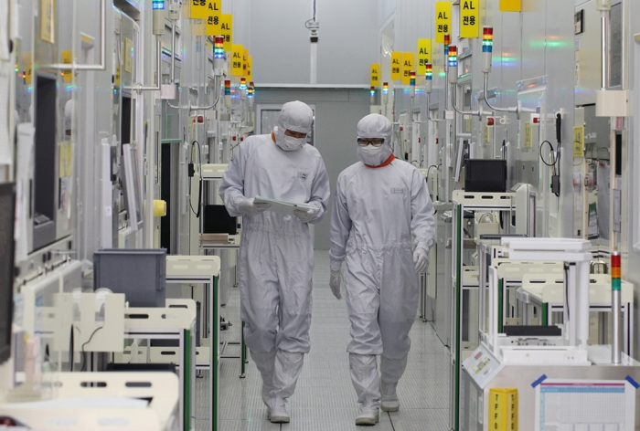
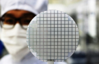
Samsung Electronics Co., the world’s largest memory chipmaker, aims to drastically expand its chip design intellectual property (IP) partnerships with its clients with a view to creating a stronger contract chipmaking ecosystem.
The move is also designed to strengthen its foundry prowess and enhance customer services to take on its archrival, Taiwan Semiconductor Manufacturing Co.
The South Korean tech giant said on Wednesday that it will beef up its semiconductor design capabilities by collaborating with leading chip design tool companies, including Synopsys, Cadence and AlphaWave Semi.
Under the plan, Samsung Foundry, the Korean firm’s contract chip manufacturing business, will provide its IP partners with foundry process information needed to develop advanced chip design technology, with which Samsung will make chips tailored to the different needs of fabless clients.
The expansion of its IP portfolio will enable Samsung to reduce errors from the early stages of design and significantly shorten the development time and cut costs of prototype production, verification and mass production.
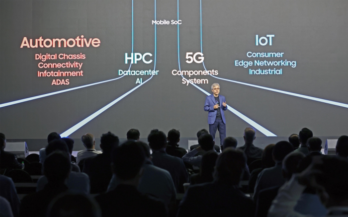
With the expanded chip design IPs, key assets for foundry players, Samsung also aims to attract new customers in fields such as artificial intelligence (AI), graphics processing units (GPUs), high-performance computing (HPC), and automotive and mobile chips.
“By actively pursuing the expansion of cutting-edge IP portfolios, we prioritize the success of our customers,” said Shin Jong-shin, vice president of Samsung’s foundry business.
NEW IP APPLICATIONS
The company said the new IPs, to be applied for process nodes from 3 nanometers to 8 nanometers, will include those for high-speed data input/output interfaces such as PCIe 6.0, 112G SerDes, DDR5/LPDDR5X/GDDR7 PHY, as well as cutting-edge UCIe IP for advanced packaging.
To strengthen its competitiveness in the automotive chip segment, Samsung plans to secure auto chip IPs that meet the highest quality standards such as AEC-Q100 and ASIL.
Samsung counts Audi, Volkswagen, BMW and Tesla among its automotive chip clients.
“The extensive IP collaboration with Samsung will enable advanced semiconductor designs, particularly for automotive, mobile and HPC applications,” said John Koeter, senior vice president of Product Management and Strategy for IP at Synopsys.
Tony Pialis, chief executive and co-founder of Alphawave Semi, said: “We are delighted to expand our state-of-the-art IP technology, which provides a new dimension of performance, flexibility and scalability to hyperscale and data infrastructure customers, to Samsung’s 3-nanometer process."
SAFE FORUM 2023
Samsung said it will unveil details of its plan to expand its IP portfolio with chip design partners as well as its advanced IP roadmap and strategies at the Samsung Advanced Foundry Ecosystem (SAFE) Forum 2023 to be held in San Jose, California June 27-28.
Samsung’s foundry business chief Choi Si-young is scheduled to give a speech on the company’s business plans on the first day of the forum.
As of 2022, the company provides more than 4,000 IPs with 56 partners. It also cooperates with nine and 22 partners in the design solution and exploratory data analysis (EDA) business, respectively.
Samsung said it works with nine partners for cloud services and 10 partners for packaging services.
Samsung, the world’s second-largest foundry player, is struggling to catch up to market leader TSMC.
According to market tracker TrendForce, the foundry market share gap between the two leading contract chipmakers widened in the first quarter from the previous quarter.
TSMC’s foundry market share rose by 1.6 percentage points to 60.1% in the January-March quarter while Samsung’s market share fell by 3.4 percentage points to 12.4%.
Samsung is striving to widen its foundry client base, from traditional fabless companies, including Qualcomm Technologies and Nvidia, to Big Tech such as Google and Microsoft, which want to make chips for their own devices.
Samsung said in December that its foundry business revenue exceeded that of its mainstay NAND flash chips – an indication that the company is gaining traction in its bid for a more significant role in the contract chip manufacturing segment.
At last year’s SAFE Forum, Samsung executives said the company aims to raise the number of its foundry clients fivefold by 2027 compared to 2019.
ARM IN TALKS WITH CLIENTS ON IPO INVESTMENT
Meanwhile, Reuters reported on Wednesday that SoftBank Group-backed UK chip design firm ARM is in talks with some of its biggest customers and end users about bringing on one or more anchor investors for its initial public offering.
ARM is in talks with at least 10 companies, including Intel, Alphabet, Apple, Microsoft, TSMC and Samsung Electronics about their potential participation in the IPO, the media outlet said.
The talks are preliminary and any decision about an anchor investment in ARM’s IPO won’t come until August, Reuters said.
ARM plans to sell its shares on the Nasdaq later this year, seeking to raise $8 billion-$10 billion.
Write to Jeong-Soo Hwang at hjs@hankyung.com
In-Soo Nam edited this article.
More to Read
-
 Korean chipmakersSystem on chips: Samsung’s new high-stakes foundry business
Mar 09, 2023 (Gmt+09:00)
2 Min read -
 Korean chipmakersSamsung eyes wider foundry client base with Ambarella deal
Feb 21, 2023 (Gmt+09:00)
2 Min read -
 Korean chipmakersSamsung’s foundry revenue exceeds mainstay NAND chip sales
Dec 13, 2022 (Gmt+09:00)
3 Min read -
 Korean chipmakersSamsung Foundry: Driving force behind digital transformation
Dec 01, 2022 (Gmt+09:00)
5 Min read -
 Korean chipmakersSamsung sets sights on GAA tech to overtake TSMC in foundry
Nov 29, 2022 (Gmt+09:00)
6 Min read -
 The KED ViewCan Samsung Electronics ever catch up to foundry leader TSMC?
May 03, 2022 (Gmt+09:00)
4 Min read
Comment 0
LOG IN