Korean chipmakers
Samsung launches next-generation chip process development unit
The move comes as Samsung shows signs of lagging in advanced chips such as HBM and DDR5 DRAM
By Nov 29, 2023 (Gmt+09:00)
4
Min read
Most Read
LG Chem to sell water filter business to Glenwood PE for $692 million


KT&G eyes overseas M&A after rejecting activist fund's offer
Kyobo Life poised to buy Japan’s SBI Group-owned savings bank
StockX in merger talks with Naver’s online reseller Kream
Meritz backs half of ex-manager’s $210 mn hedge fund


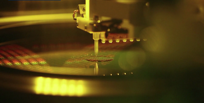
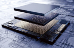
Samsung Electronics Co., the world’s largest memory chipmaker, has launched a business unit tasked with developing next-generation chip processing technology as the company aims to take the lead in the artificial intelligence (AI) chip segment.
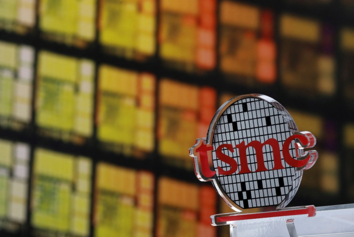
Industry sources said on Wednesday Samsung recently set up the division to develop new technology to stay ahead of its rivals, including foundry leader Taiwan Semiconductor Manufacturing Co. (TSMC), at the leading edge of chip processing.
The new unit will be led by Hyun Sang-jin, a vice president-level researcher who was promoted to president on Wednesday, sources said.
Hyun is credited with his critical role in Samsung’s tech advancement in semiconductor process nodes and mass production of its advanced 3-nanometer chips.
The unit will be placed under Samsung’s chip research center within its Device Solutions (DS) division, which oversees its semiconductor business, they said.
“Samsung wants to develop new technologies that will put it ahead of its rivals over the next decade or two,” said one of the people.
The Suwon, South Korea-based company hopes to have developed tech deemed a game changer – something similar to its gate-all-around, or GAA, technology unveiled last year.
The GAA architecture, a next-generation foundry microfabrication process, is a key technology that improves electrostatic properties that translate into increased performance, reduced power and optimal chip designs.
Samsung said the 3 nm GAA technology offers a 30% performance boost, a 50% decrease in energy consumption and a 45% reduction in chip area, compared to the previous processing node.
The GAA tech competes with TSMC and other foundry companies that use a technology called the fin field-effect transistor (FinFET) process. Since its structure resembles a fish’s dorsal fin, it is also called the fin transistor.
Although Samsung is the No. 1 memory chipmaker, it lags far behind TSMC in the foundry or contract chipmaking segment in terms of market share.
TO MOVE CHIP PACKAGING TECH UNIT CLOSER TO SEOUL
Samsung also plans to move its chip packaging technology development unit to Yongin or Hwaseong, south of Seoul, where its main chip production cluster is located, from Cheonan in South Chungcheong Province.
As the AVP Business team in charge of developing advanced chip packaging tech at its Cheonan research center is located relatively far from Seoul, talented researchers in Seoul and the surrounding metropolitan area are reluctant to move there to work, industry officials said.
Packaging, one of the final steps in semiconductor manufacturing, places chips in a protective case to prevent corrosion and provides an interface to combine and connect already-made chips.
Leading chipmakers such as TSMC, Samsung and Intel Corp. are fiercely competing for advanced packaging to enhance chip performance without having to shrink the nanometer through ultra-fine processing, which is technologically challenging and requires more time.
Earlier this month, sources said Samsung plans to unveil an advanced three-dimensional (3D) chip packaging technology next year to better compete with its rivals.
The technology, dubbed SAINT, or Samsung Advanced Interconnection Technology, will integrate memory and processors required of high-performance chips, including AI chips, in much smaller sizes, sources said.
FALTERING TECH LEADERSHIP
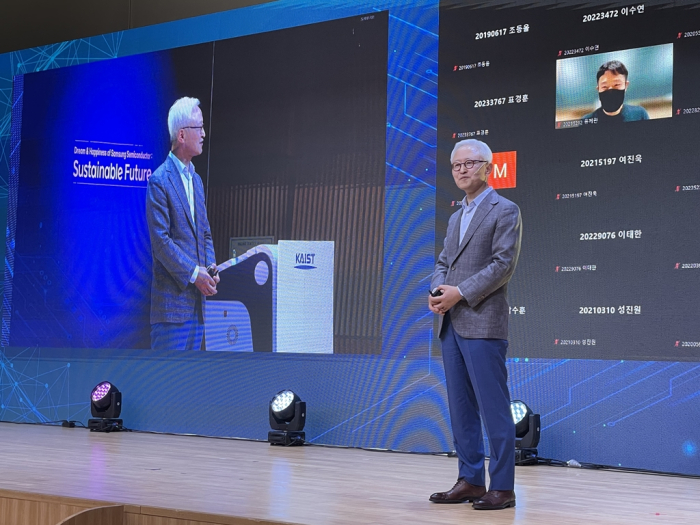
Industry officials said the establishment of a new chip process tech development unit at Samsung was led by Kyung Kye-hyun, chief of the company’s semiconductor business.
In a C-suite executive reshuffle on Monday, Kyung retained his post as co-CEO and chief of the DS division. In addition, he was named to head the company’s top research center, the Samsung Advanced Institute of Technology (SAIT).
The launch of the new unit is part of Samsung’s push to lead in the AI chip segment, which, according to Gartner, is forecast to grow to $119.4 billion by 2027 from an estimated $53.4 billion this year.
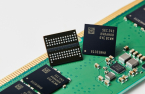
However, Samsung has fallen behind its crosstown rival SK Hynix Inc. in advanced memory chip markets such as high bandwidth memory (HBM) and double data rate5 (DDR5) DRAM.
HBM is a high-capacity, high-performance semiconductor chip, demand for which is soaring as it is used to power generative AI devices like ChatGPT, high-performance data centers and machine learning platforms.
As Samsung’s business focus expanded from memory chips to foundry and chip design, its investment resources, including talented researchers, for more advanced chip process technology have been dispersed, industry officials said.
Write to Jeong-Soo Hwang at hjs@hankyung.com
In-Soo Nam edited this article.
More to Read
-
 Executive reshufflesSamsung sets up future business planning unit, keeps co-CEO system
Nov 27, 2023 (Gmt+09:00)
4 Min read -
 Korean chipmakersSamsung to unveil 3D AI chip packaging tech SAINT to rival TSMC
Nov 12, 2023 (Gmt+09:00)
3 Min read -
 Korean chipmakersSamsung Elec to launch HBM4 in 2025 to win war in AI sector
Oct 10, 2023 (Gmt+09:00)
2 Min read -
 Korean chipmakersSamsung set to supply HBM3 to Nvidia, develops 32 Gb DDR5 chip
Sep 01, 2023 (Gmt+09:00)
4 Min read -
 Korean chipmakersSamsung rolls out industry’s finest 12 nm DDR5 DRAM chips
May 18, 2023 (Gmt+09:00)
3 Min read -
 Korean chipmakersSamsung sets sights on GAA tech to overtake TSMC in foundry
Nov 29, 2022 (Gmt+09:00)
6 Min read -
 Korean chipmakersSamsung to make 2-nanometer GAA chips by 2025 to overtake TSMC
Oct 07, 2021 (Gmt+09:00)
3 Min read
Comment 0
LOG IN