Korean chipmakers
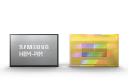
Samsung Elec to launch HBM4 in 2025 to win war in AI sector
The Korean tech giant is developing the sixth-gen HBM model while planning to supply fifth-gen HBM3E samples
By Oct 10, 2023 (Gmt+09:00)
2
Min read
Most Read
Hankook Tire buys $1 bn Hanon Systems stake from Hahn & Co.


NPS to hike risky asset purchases under simplified allocation system
Osstem to buy BrazilŌĆÖs No. 3 dental implant maker Implacil
UAE to invest up to $1 bn in S.Korean ventures
US multifamily market challenges create investment opportunities


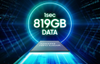
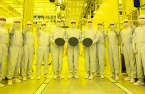
Samsung Electronics Co., the worldŌĆÖs top memory chipmaker, aims to introduce sixth-generation top-performance High Bandwidth Memory4 (HBM4) DRAM chips in 2025 to win the intensifying battle for dominance in the fast-growing artificial intelligence chip segment, an executive of the company said on Tuesday.
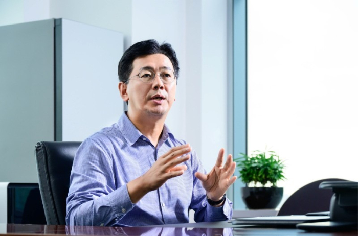
Hwang Sang-joon, executive vice president of DRAM product & technology at Samsung, said the company is developing the product while planning to supply samples of the fifth-generation HBM3E to customers.
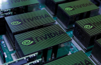
HBM is a high-capacity, high-performance semiconductor chip, demand for which is soaring as it is used to power generative AI devices like ChatGPT, high-performance data centers and machine learning platforms.
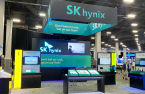
Samsung has been in cut-throat competition against its smaller domestic rival SK Hynix Inc. for dominance in the sector.
ŌĆ£Samsung commercialized HBM for high-performance computing (HPC) in 2016 for the first time in the world,ŌĆØ Hwang said in a contribution to Samsung Newsroom, the companyŌĆÖs public relations website. ŌĆ£We pioneered the AI memory chip market while mass-producing second- to fourth-generation HBM products.ŌĆØ
The South Korean tech giant aims to lead the AI chip market with its semiconductor turnkey service, which includes foundry, memory chip supplies, advanced packaging and tests.
ŌĆ£We are providing customized turnkey services such as the cutting-edge 2.5D and 3D packaging along with HBM,ŌĆØ Hwang said. ŌĆ£We will offer the best service for the AI and HPC era.ŌĆØ
FUTURE MEMORY CHIP BUSINESS
Hwang unveiled a blueprint for the future memory chip business including computer express link (CXL) DRAM and processing-in-memory (PIM).
CXL is a next-generation interface that adds efficiency to accelerators, DRAM and storage devices used with central processing units (CPUs) in high-performance server systems. PIM is a DRAM that helps process data like a CPU.
ŌĆ£Memory bottlenecks are fatal for devices, which handle massive data like ChatGPT,ŌĆØ Hwan said. ŌĆ£The HBM-PIM we have recently developed eased bottlenecks of data bandwidth while increasing work performance by 12 times.ŌĆØ
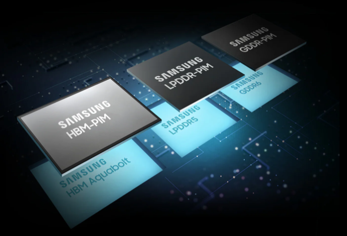
The company is also working on the construction of PIM structure on CXL DRAMs, he added.
Hwang has high hopes for a low-power compression attached memory module (LPCAMM) unveiled last month. The LPCAMM is a more advanced memory form factor built upon a package of multiple low-power double data rate (LPDDR) memory chips, the industryŌĆÖs first of its kind.
ŌĆ£The LPCAMM will help make laptops and other devices thinner as it needs up to 60% narrower space for installation than the existing products,ŌĆØ he said. ŌĆ£Its performance and power efficiency improved by as much as 50% and 70%, respectively. So, it will be used not only for laptops but also for data centers.ŌĆØ
Samsung plans to use processing technologies of below 10 nanometers, the inflection point of the global DRAM market, in the future, he said.
ŌĆ£We will provide memory products of ultra-high performance, ultra-high capacity and ultra-low power consumption that the world wants in the AI era.ŌĆØ
Write to Ik-Hwan Kim at lovepen@hankyung.com
┬Ā
Jongwoo Cheon edited this article.
More to Read
-
 Korean chipmakersSamsung set to keep supremacy in low power DRAM with game changer
Sep 26, 2023 (Gmt+09:00)
2 Min read -
 Korean chipmakersHBM chips key theme for Samsung Nov investors forum
Sep 15, 2023 (Gmt+09:00)
2 Min read -
 Korean chipmakersSK Hynix, Samsung's fight for HBM lead set to escalate on AI boom
Sep 03, 2023 (Gmt+09:00)
4 Min read -
 Korean chipmakersSamsung set to supply HBM3 to Nvidia, develops 32 Gb DDR5 chip
Sep 01, 2023 (Gmt+09:00)
4 Min read -
 Korean chipmakersSamsung set to supply HBM3, packaging services to AMD
Aug 22, 2023 (Gmt+09:00)
1 Min read -
 Korean chipmakersSamsung Elec launches foundry package turnkey service
Apr 14, 2023 (Gmt+09:00)
3 Min read
Comment 0
LOG IN