Korean chipmakers
Samsung Electronics to overtake TSMC within 5 years: chip president
Once TSMC joins the race for the 2-nanometer process node based on GAA technology, Samsung can lead the way, he says
By May 04, 2023 (Gmt+09:00)
3
Min read
Most Read
LG Chem to sell water filter business to Glenwood PE for $692 million


KT&G eyes overseas M&A after rejecting activist fund's offer
Kyobo Life poised to buy Japan’s SBI Group-owned savings bank
StockX in merger talks with Naver’s online reseller Kream
Meritz backs half of ex-manager’s $210 mn hedge fund


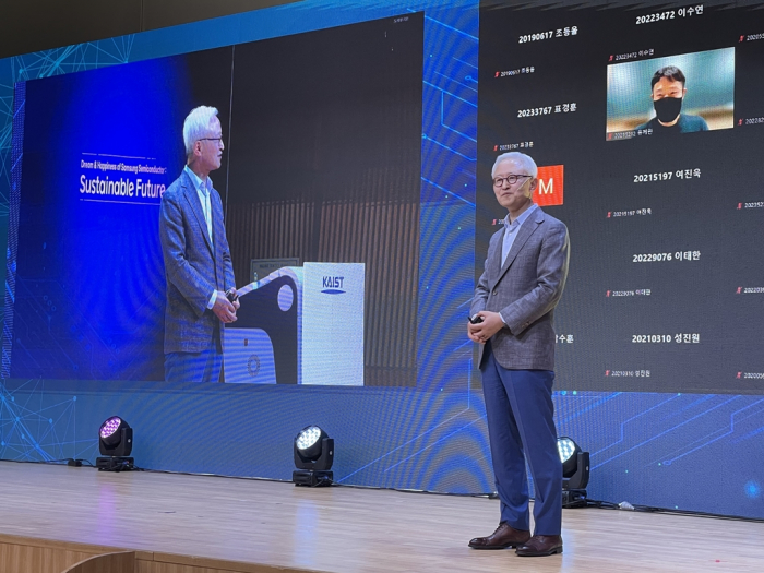
DAEJEON – Samsung Electronics Co. will be able to overtake bigger foundry rival Taiwan Semiconductor Manufacturing Co. (TSMC) at the leading edge of chip processing within five years, its chip business leader said on Friday.
While Samsung is currently behind TSMC in chip processing technology, it expects to get ahead of the Taiwanese company from the 2-nanometer processing node, he said.
“To be honest, our foundry technology is one or two years behind TSMC’s. However, once TSMC joins us in the race for 2-nanometer technology, Samsung will lead the way,” Kyung Kye-hyun, president and head of Samsung’s semiconductor business, said at a lecture at KAIST, one of South Korea’s top science and technology institutes. “Within five years, we can surpass TSMC.”
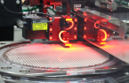
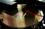
Last year, Samsung, as a global first, applied a 3 nm process node to the manufacture of advanced chips based on the gate-all-around (GAA) transistor architecture.
The GAA architecture, a next-generation foundry microfabrication process, is a key technology that improves electrostatic properties that translate into increased performance, reduced power and optimal chip designs.
Samsung said the 3 nm GAA technology offers a 30% performance boost, a 50% decrease in energy consumption and a 45% reduction in chip area, compared to the previous processing node.
Samsung earlier said it aims to mass produce 2 nm chips based on the GAA architecture from 2025.
TSMC and other foundry companies use a technology called fin field-effect transistor (FinFET) process. Since its structure resembles a fish’s dorsal fin, it is also called the fin transistor.
TSMC, the foundry market leader, reportedly plans to apply GAA technology to its chip manufacturing process from the 2 nm node.
“Samsung's 4 nm technology is two years behind TSMC's, and our 3 nm is about a year behind. But things will change when TSMC enters the 2 nm process," Kyung said.
"Our customers are favorable to our GAA technology. Almost all major companies are working with us, although I can't disclose their names. Samsung's foundry customer base is growing,” he said.
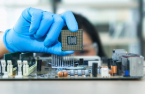
Samsung is the world’s largest memory chipmaker but lags far behind TSMC in the foundry or contract chipmaking segment in terms of market share.
PACKAGING TECHNOLOGY
Kyung said Samsung is also trying to advance its chip packaging technology to stay ahead of its rivals.
"As semiconductor process miniaturization becomes more difficult, performance will ultimately be improved through packaging,” he said.
Samsung launched an advanced packaging team last year and the company expects a significant improvement within three to four years, he said.
The Samsung executive also said the importance of memory chips in artificial intelligence (AI) servers will exceed that of Nvidia Corp.’s graphics processing unit (GPU) in the near future.
“We will make it possible for a supercomputer that is centered around memory semiconductors to emerge by 2028,” he said.
IN CHINA, SAMSUNG CAN STAND
Regarding the tightening of US rules on chipmakers’ operations in China, he said Samsung can stand.
"While approval is required for investment in our Chinese plant in Xian, I don't think there will be any significant pressure on our overall business," he said. "We will strive to turn the crisis into an opportunity."
The escalating Washington-Beijing semiconductor rivalry is posing a risk to global chipmakers, including Samsung and its crosstown rival SK Hynix Inc.
In its efforts to wean Korean chipmakers off Chinese dependence, a senior US government official said in February it may put a cap on technology levels that Samsung and SK Hynix could grow to in China.
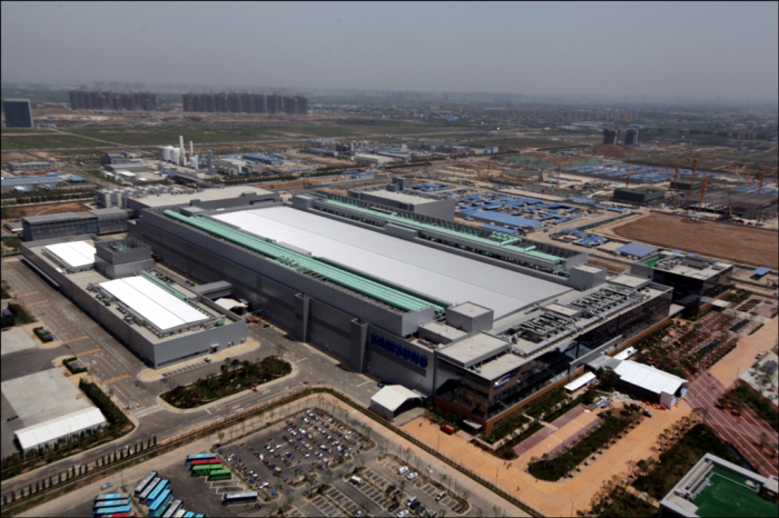
In China, the Korean chipmaker operates a NAND flash memory plant in Xian and a chip packaging facility in Suzhou.
Samsung’s Xian plant accounts for nearly 40% of the company’s entire NAND production globally. The company has invested $25.8 billion in its Xian plant since 2021.
Last year, Samsung posted 35.63 trillion won ($27.2 billion) in sales revenue from its Chinese operations.
Write to Ye-Rin Choi at rambutan@hankyung.com
In-Soo Nam edited this article.
More to Read
-
 Korean chipmakersSamsung sets sights on GAA tech to overtake TSMC in foundry
Nov 29, 2022 (Gmt+09:00)
6 Min read -
 Korean chipmakersSamsung unveils 1.4-nano tech roadmap to challenge TSMC’s dominance
Oct 04, 2022 (Gmt+09:00)
4 Min read -
 The KED ViewCan Samsung Electronics ever catch up to foundry leader TSMC?
May 03, 2022 (Gmt+09:00)
4 Min read -
 Korean chipmakersSamsung’s $17 billion new chip plant in Taylor aims to rein in TSMC
Nov 24, 2021 (Gmt+09:00)
4 Min read -
 Korean chipmakersSamsung to make 2-nanometer GAA chips by 2025 to overtake TSMC
Oct 07, 2021 (Gmt+09:00)
3 Min read
Comment 0
LOG IN