Korean chipmakers
Samsung unveils 1.4 nm tech roadmap to challenge TSMC’s dominance
Samsung also aims to triple its chip production capacity by 2027 and introduce a ‘shell-first’ operation strategy
By Oct 04, 2022 (Gmt+09:00)
4
Min read
Most Read
LG Chem to sell water filter business to Glenwood PE for $692 million


KT&G eyes overseas M&A after rejecting activist fund's offer
Kyobo Life poised to buy Japan’s SBI Group-owned savings bank
StockX in merger talks with Naver’s online reseller Kream
Meritz backs half of ex-manager’s $210 mn hedge fund


SILICON VALLEY – Samsung Electronics Co. said on Monday it will adopt the industry’s most advanced 1.4-nanometer chip production technology by 2027 to take on bigger foundry rival Taiwan Semiconductor Manufacturing Co. at the leading edge of chip processing.
At the Samsung Foundry Forum 2022, the South Korean tech giant also said it will ensure non-mobile applications such as high-performance computing (HPC), 5G connectivity and automotive chips account for more than half of its foundry sales by then to diversify its business portfolio.
During the forum, an annual gathering of the chipmaker’s clients and partners, Samsung’s foundry business chief Choi Si-young said the company will start manufacturing chips on the 2 nm node in 2025 and move on to a more advanced 1.4 nm process in 2027.
Samsung said it is the industry’s first to unveil the advanced chip processing technology roadmap ahead of foundry leader TSMC.
In May, TSMC said it will launch a 1.4 nm process without providing a specific timeline. The market expects the Taiwanese company to introduce advanced tech around 2027 or 2028.
In the chipmaking process, nanometer refers to the circuitry size of the transistors that can be packed on a chip. The lower the nanometer number, the more advanced the technology, promising a faster computing speed, higher performance and lower power use.
“The technology development goal down to 1.4 nanometers and foundry platforms specialized for each application, together with stable supply through consistent investment are all part of Samsung’s strategy to secure customers’ trust and support their success,” Choi said at the Samsung forum.
TECH RACE GOING INTO HIGH GEAR
The competition between the world’s two largest contract chipmakers is going into high gear at a time when their clients such as US tech giant Intel Corp. have also thrown down the gauntlet to jump into the fast-growing foundry business.
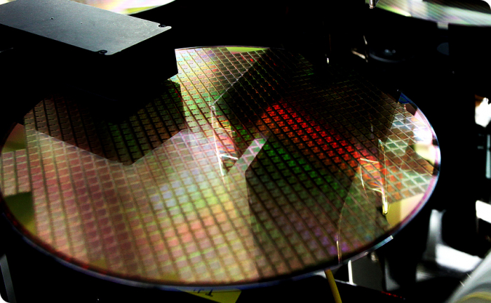
Samsung and TSMC have already been producing chips with 3 nm processing nodes, although the two rivals use different technologies.
Samsung’s production tech is based on its proprietary gate-all-around (GAA) transistor architecture, a next-generation foundry microfabrication process.
The company said its 3 nm GAA offers a 30% performance boost, a 50% decrease in energy consumption and a 35% reduction in chip area, compared to the 5 nm process.
Meanwhile, TSMC’s 3 nm process node is based on a technology called fin field-effect transistor (FinFET) process.
The two companies have been upping the ante to stay ahead by aggressively expanding facilities and engaging in a closely watched technology race.
Samsung is the world’s top memory chipmaker. In the contract manufacturing business, however, it is a distant second with a low double-digit market share after TSMC, which controls more than half of the global foundry market.
According to market researcher TrendForce, Samsung’s foundry business posted $5.59 billion in sales revenue in the second quarter.
“SHELL-FIRST” OPERATION STRATEGY
With its more advanced nodes, Samsung said on Monday it aims to more than triple its advanced chip production capacity by 2027 compared to this year.
It also said it will introduce a “shell-first” operation strategy for capacity expansion, meaning building cleanrooms first irrespective of market conditions to swiftly respond to customer demand.
With cleanrooms readily available, fab equipment can be installed later and set up flexibly as needed in line with future demand, it said.
“Foundry is like a hotel business. We’re changing our business style to build rooms before welcoming our customers,” said Kyung Kye-hyun, president of Samsung’s device solution division, which is in charge of Samsung’s entire semiconductor business.
The move comes as Samsung is widening its foundry client base from Qualcomm and Nvidia to Google and Tesla.
Samsung plans to first apply the shell-first strategy to the second line of its new $17 billion foundry plant under construction in Taylor, Texas.
Samsung has contract chipmaking facilities in five locations around the world: Giheung, Hwaseong and Pyeongtaek in Korea; and Austin and Taylor in the US.
According to market research firm Omdia, the 5 nm and narrower chip processing market is forecast to grow at an annual average rate of 98% to $53.85 billion by 2025 from $19.45 billion in 2022.
Write to Ki-Yeol Seo, Jeong-Soo Hwang and Sungsu Bae at philos@hankyung.com
In-Soo Nam edited this article.
More to Read
-
 Korean chipmakersSamsung nears 3-nano chip mass production ahead of TSMC
Jun 28, 2022 (Gmt+09:00)
3 Min read -
 The KED ViewCan Samsung Electronics ever catch up to foundry leader TSMC?
May 03, 2022 (Gmt+09:00)
4 Min read -
 Korean chipmakersSamsung to make 2-nanometer GAA chips by 2025 to overtake TSMC
Oct 07, 2021 (Gmt+09:00)
3 Min read -
 Korean chipmakersSamsung overtakes Intel as foundry looms as next battlefield
Aug 02, 2021 (Gmt+09:00)
3 Min read -
 Korean chipmakersSamsung loses ground in foundry market as TSMC ties in with Japanese firms
Jun 01, 2021 (Gmt+09:00)
2 Min read -
 Korean chipmakersSamsung, TSMC up ante in US foundry competition
May 24, 2021 (Gmt+09:00)
3 Min read
Comment 0
LOG IN