Korean chipmakers
Samsung wins 2nm AI chip foundry, package order from Japan
The chipmaker will further advance its foundry process to the 1.4nm node by 2027, its foundry chief says
By Jul 09, 2024 (Gmt+09:00)
3
Min read
Most Read
LG Chem to sell water filter business to Glenwood PE for $692 million


KT&G eyes overseas M&A after rejecting activist fund's offer
Kyobo Life poised to buy Japan’s SBI Group-owned savings bank
StockX in merger talks with Naver’s online reseller Kream
Meritz backs half of ex-manager’s $210 mn hedge fund


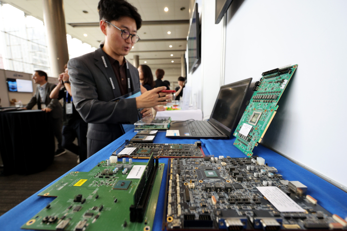
Samsung Electronics Co. announced on Tuesday it has bagged a 2-nanometer AI chip foundry and package turnkey order from Preferred Networks Inc., a Japanese AI application developer, a deal the world’s No. 1 memory chipmaker said would help expand South Korea’s foundry ecosystem.
Under the contract, Samsung will manufacture AI accelerators using the 2nm foundry process based on its proprietary Gate-All-Around (GAA) technology and the advanced 2.5-dimensional packaging service. It did not disclose the deal size.
Gaonchips Co., a domestic fabless company, designs the accelerator.
Samsung flagged the foundry and packaging service order as the outcome of its collaboration with domestic chip designers aimed at strengthening the country’s foundry market.
Other domestic fabless startups such as Telechips, ABOV Semiconductor and Rebellions Inc. have outsourced chip manufacturing to Samsung. They are expanding their partnership to develop next-generation AI chips.
“This order is pivotal as it validates Samsung’s 2nm GAA process technology and advanced package technology as an ideal solution for next-generation AI accelerators,” Song Taejoong, corporate vice president and the head of Samsung’s foundry business development team, said in a press release.
Last year, Samsung launched the package turnkey service that handles the entire chip packaging process from production to testing for fabless companies.
In 2022, it started mass production of chips based on the GAA foundry technology for the first time in the world.

ONE-STOP AI SOLUTIONS
Samsung will deepen collaboration with Preferred Networks to develop groundbreaking AI chiplets for use in next-generation data centers and generative AI computing systems, Samsung added.
Chiplet solution refers to assembling multiple chips into a single package.
The 2.5D advanced packaging is a heterogeneous integration package technology with different types of chips such as memory, logic and sensors packed in one package to enhance interconnection speed and reduce packaging size.
Samsung revealed the order received from Preferred Networks at Samsung Foundry Forum 2024 and Samsung Advanced Foundry Ecosystem (SAFE) Forum 2024 held at COEX, Seoul on Tuesday.
SF2Z FOR CHIP MASS PRODUCTION IN 2027
Last month, Samsung reaffirmed its plan to mass-produce the 2nm process for mobile applications in 2025 before expanding to other uses later.
It also showcased two upgraded process nodes, SF2Z and SF4U. Mass production using the new SF2Z tech is slated for 2027, Choi Siyoung, Samsung's foundry chief, said at the foundry forum.
SF2Z incorporates optimized backside power delivery network (BSPDN) technology, which places power rails on the backside of the wafer to eliminate bottlenecks between the power and signal lines.
1.4 NANO PROCESS
Samsung will further advance its foundry process to the cutting-edge 1.4nm node by 2027, said Choi.
“We are breaking through the limits of miniaturization and preparing for new technological innovations through cooperation with various companies,” he added.
16-LAYER HBM4
Choi Jang-seok, executive director of Samsung’s memory division, said it is developing 16-layer HBM4 chips according to schedule. High-bandwidth memory (HBM) is essential for generative AI thanks to its fast processing of vast amounts of data.
Samsung will launch 3D packaging services for HBM this year for the HBM4 model due in 2025, according to the company and industry sources last month.
Rebellions is developing next-generation AI accelerators based on Samsung’s 4nm process shifting from the chipmaker’s 5nm node, said Oh Jinwook, Rebellions' chief technology officer.
ABOV Semiconductor is producing non-volatile memory, a core component of microcontroller units, using Samsung’s 65nm process, said its Vice President Park Ho-jin. This year, it will produce advanced chips based on Samsung’s 28nm process.
Samsung will also host Samsung Foundry Forum 2024 in Japan and Europe in the second half of this year.
Write to Jeong-Soo Hwang at hjs@hankyung.com
Yeonhee Kim edited this article.
More to Read
-
 Korean chipmakersHBM chip war intensifies as SK Hynix hunts for Samsung talent
Jul 08, 2024 (Gmt+09:00)
4 Min read -
 Korean chipmakersSamsung launches dedicated HBM, advanced chip packaging teams
Jul 05, 2024 (Gmt+09:00)
3 Min read -
 EarningsSamsung’s Q2 profit soars on AI chips; second-half outlook rosy
Jul 05, 2024 (Gmt+09:00)
3 Min read -
 Korean chipmakersKorea to inject $200 mn into semiconductor packaging R&D
Jun 26, 2024 (Gmt+09:00)
2 Min read -
 Korean chipmakersSamsung to launch 3D HBM chip packaging service in 2024
Jun 16, 2024 (Gmt+09:00)
2 Min read -
 Korean chipmakersSamsung unveils new foundry tech; AI chip sales to rise ninefold
Jun 13, 2024 (Gmt+09:00)
4 Min read -
 Korean chipmakersSamsung Elec launches foundry package turnkey service
Apr 14, 2023 (Gmt+09:00)
3 Min read
Comment 0
LOG IN