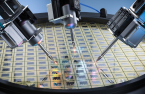
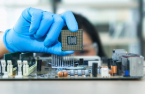
Samsung unveils new foundry tech; AI chip sales to rise ninefold
Samsung says its GAA process is consistently demonstrating improvements in yield and performance
By Jun 13, 2024 (Gmt+09:00)
LG Chem to sell water filter business to Glenwood PE for $692 million


KT&G eyes overseas M&A after rejecting activist fund's offer
Kyobo Life poised to buy Japan’s SBI Group-owned savings bank
StockX in merger talks with Naver’s online reseller Kream
Meritz backs half of ex-manager’s $210 mn hedge fund


SAN JOSE, Calif. – Samsung Electronics Co., the world’s largest memory chipmaker, on Wednesday unveiled a new contract chipmaking technology, with which it aims to raise its artificial intelligence chip sales ninefold by 2028.
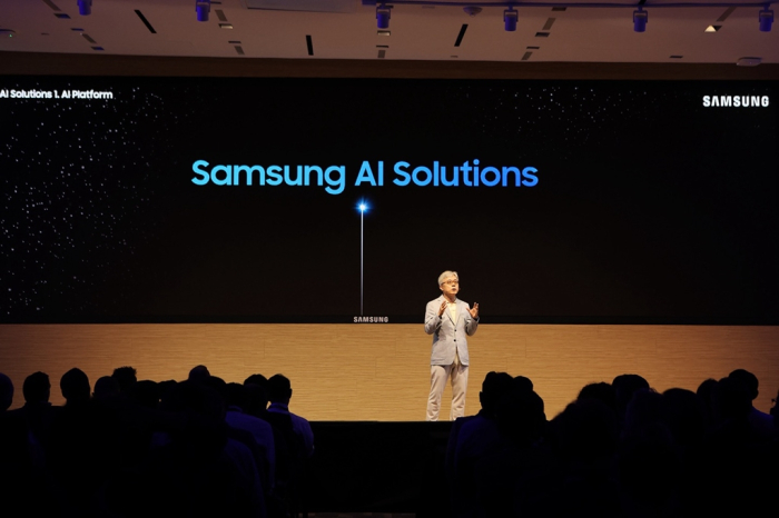
“At a time when numerous technologies are evolving around AI, the key to its implementation lies in high-performance, low-power semiconductors,” said Choi Si-young, Samsung’s foundry business chief, at the Samsung Foundry Forum (SFF) 2024.
“Alongside our proven GAA process optimized for AI chips, we plan to introduce integrated, co-packaged optics technology for high-speed, low-power data processing, providing our customers with the one-stop AI solutions they need to thrive in this transformative era.”
At this year’s annual foundry forum in San Jose, California, Samsung reaffirmed its plan to begin mass production of the 2-nanometer process for mobile applications in 2025 before expanding to other uses in later years.
It said it will apply the advanced 2 nm tech to high-performance computing (HPC) chips for supercomputers and computer clusters in 2026 and then to automotive chips in 2027.
Samsung also confirmed its plans to begin mass production of more advanced 1.4 nm chips by 2027.
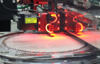
BACKSIDE POWER DELIVERY NETWORK (BSPDN) TECH
At Wednesday’s event, Samsung showcased two upgraded process nodes, SF2Z and SF4U, reinforcing its cutting-edge process tech roadmap.
What’s notable about the SF2Z node is that it incorporates backside power delivery network (BSPDN) technology, which places power rails on the back of the wafer to eliminate bottlenecks between the power and signal lines.
Applying BSPDN tech to SF2Z not only enhances power, performance and area (PPA) compared to SF2, the first-generation 2 nm node, but also significantly reduces voltage drop, enhancing the performance of HPC design, Samsung said.
Mass production using the new SF2Z tech is slated for 2027, it said.
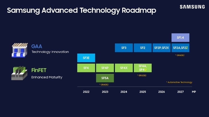
SF4U, a 4 nm variant that offers PPA improvements by incorporating optical shrink, will begin mass production in 2025, it said.
TSMC, which controls 62% of the global foundry market, said it plans to introduce the BSPDN tech to its 1.6 nm and below process nodes around the end of 2026.
SAMSUNG’S GAA TECH ADVANCED
With the onset of the AI era, structural advancements such as Samsung’s gate-all-around (GAA) tech have become crucial to meeting power and performance demands.
At SFF 2024, Samsung said its GAA process is consistently demonstrating improvements in yields and performance.
“Leveraging this accumulated GAA production experience, Samsung plans to mass-produce its second-generation 3 nm process (SF3) in the second half of this year and deliver GAA on its upcoming 2 nm process,” it said.
With demand for high-performance chips rising, competition for technology advancement is also fierce, particularly between foundry leader TSMC and fast-follower Samsung.
While Samsung’s production tech is based on GAA transistor architecture for its microfabrication process, TSMC uses a different technology in the fin field-effect transistor (FinFET) structure.
SAMSUNG EXPECTS AI CHIP SALES TO RISE NINEFOLD
Samsung Vice President Song Tae-joong said during a media briefing at SFF 2024 that the company expects its AI chip sales to rise by 1.8 times this year from last year and increase ninefold by 2028.
“We keep receiving orders for AI chips,” he said.

Samsung’s AI chip clients will double this year and rise fourfold by 2028, he said.
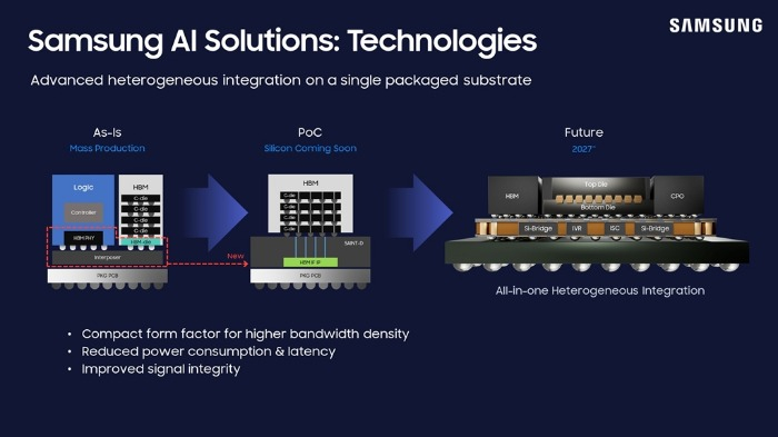
Samsung said it will introduce an all-in-one integrated turnkey AI platform by 2027 to provide customers with “one-stop AI solutions.”
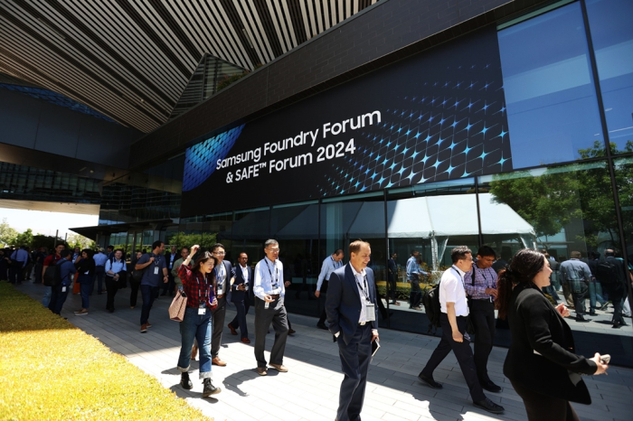
In San Jose, Samsung also hosts Samsung Advanced Foundry Ecosystem (SAFE) Forum 2024 and an inaugural Multi-Die Integration (MDI) Alliance workshop with its partner companies to create new, customized packaging technologies for applications in the HPC and automotive industries.
Industry leaders joining this year’s forum included Arm Chief Executive Rene Haas, Groq CEO Jonathan Ross, Siemens CEO Mike Ellow, AMD Vice President Bill En and Celestial AI CEO David Lazovsky.
Write to Jeong-Soo Hwang and Jin-Suk Choi at hjs@hankyung.com
In-Soo Nam edited this article.
-
 Korean chipmakersSamsung, AMD to collaborate on 3 nm GAA tech chipmaking
May 29, 2024 (Gmt+09:00)
2 Min read -
 Korean chipmakersSamsung wins first 2 nm AI chip order from Japan’s PFN; a snub to TSMC
Feb 16, 2024 (Gmt+09:00)
3 Min read -
 Korean chipmakersSamsung on smooth track to 1.4 nm foundry tech to take on TSMC
Jun 28, 2023 (Gmt+09:00)
4 Min read -
 Korean chipmakersSamsung sets sights on GAA tech to overtake TSMC in foundry
Nov 29, 2022 (Gmt+09:00)
6 Min read -
 Korean chipmakersSamsung to make 2-nanometer GAA chips by 2025 to overtake TSMC
Oct 07, 2021 (Gmt+09:00)
3 Min read