Korean chipmakers
Samsung to unveil Mach-1 AI chip to upend SK Hynix’s HBM leadership
A laggard in the sought-after HBM chips, Samsung aims to become the top AI chipmaker within a couple of years
By Mar 20, 2024 (Gmt+09:00)
3
Min read
Most Read
LG Chem to sell water filter business to Glenwood PE for $692 million


KT&G eyes overseas M&A after rejecting activist fund's offer
Kyobo Life poised to buy Japan’s SBI Group-owned savings bank
StockX in merger talks with Naver’s online reseller Kream
Meritz backs half of ex-manager’s $210 mn hedge fund


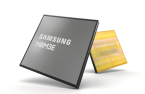
Samsung Electronics Co., the world’s top memory chipmaker, is developing a next-generation artificial intelligence chip, Mach-1, with which the South Korean tech giant aims to upend its crosstown rival SK Hynix Inc., the dominant player in the advanced high bandwidth memory (HBM) segment.
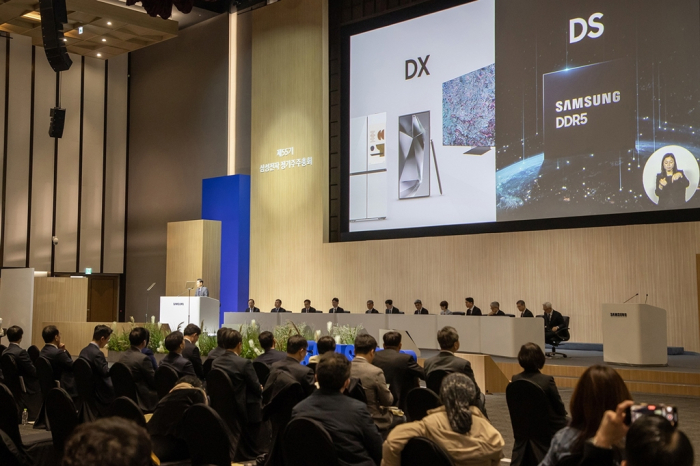
Kyung Kye-hyun, head of Samsung's semiconductor business, said on Wednesday the Mach-1 AI chip is currently under development and the company plans to produce a prototype by year-end.
“The current AI systems have performance degradation and power issues due to memory bottlenecks. We will address this problem by establishing an AGI computing lab and achieving AI architecture innovation. Mach-1 is at the center of our R&D efforts,” he said at Samsung’s annual general meeting held in Suwon, west of Seoul, where its headquarters is based.
AGI, short for artificial general intelligence, is a type of AI that can perform as well or better than humans on a wide range of cognitive tasks.
Industry officials said it is the first time for the Samsung semiconductor chief to make public its development of a next-generation AI chip.

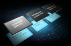
Mach-1 is an AI accelerator in the form of a system-on-chip (SoC) that reduces the bottleneck between the graphics processing unit (GPU) and HBM chips, according to Samsung.
“It is a product specified to fit the transformer model. By using several algorithms, we aim to reduce the bottleneck phenomenon that occurs between memory and GPU chips to one-eighth of what we’re witnessing today and improve the power efficiency by eight times,” he said.
“It (Mach-1) will enable large language model (LLM) inference even with low-power memory instead of power-hungry HBM.”
SAMSUNG AIMS TO UNSEAT SK HYNIX IN HBM LEADERSHIP
Kyung, chief executive of Samsung’s Device Solutions (DS) division, which oversees its chip business, said the technical verification of the Mach-1 chip has already been done through integrated circuits, called field programmable gate arrays (FPGAs), and an SoC design work for Mach-1 is underway.

FPGA circuits are referred to as 'field programmable' because they allow customers to reconfigure the hardware to meet specific use case requirements after the manufacturing process.
“We will make prototype (Mach-1) chips by the end of this year. Then, we will see AI systems using our latest AI chips early next year,” he said.
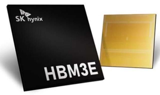
With the new AI chip, analysts said, Samsung aims to catch up with rival SK Hynix, which recently started mass production of its next-generation HBM chip.
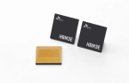
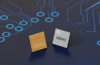
HBM has become an essential part of the AI boom, as it provides the much-needed faster processing speed compared with traditional memory chips.
A laggard in the HBM chip segment, Samsung has been investing heavily in HBM to rival SK Hynix and other memory players.
Last month, Samsung said it developed HBM3E 12H, the industry's first 12-stack HBM3E DRAM and the highest-capacity HBM product to date. Samsung said that it will start mass production of the chip in the first half of this year.
TO INVEST $15 BILLION IN R&D TO BECOME TOP CHIPMAKER
At the shareholders’ meeting, Kyung said he expects more than $1 billion in sales from its advanced chip packaging business this year.
Asked if Samsung has an intention to take its chip packaging business globally, he said nothing concrete has been decided yet.
Last December, it said it would build a 40 billion yen ($281 million) advanced chip packaging R&D center in Yokohama, southwest of Tokyo, to develop new chip packaging technology and deepen ties with Japanese makers of chipmaking equipment and materials.
Samsung said on Wednesday it will invest 20 trillion won ($15 billion) in its R&D complex in Giheung, Korea by 2030 as part of its goal to become the world’s No. semiconductor maker.
According to market tracker Gartner, Intel Corp. was the world’s top chipmaker last year with sales revenue of $48.7 billion, followed by Samsung with sales of $39.9 billion, down 37.5% from the year prior.
“We will regain the No. 1 spot within the next two to three years,” Kyung said.
Write to Chae-Yeon Kim and Jeong-Soo Hwang at why29@hankyung.com
In-Soo Nam edited this article.
More to Read
-
 Korean chipmakersSamsung rallies on expectations of Nvidia’s HBM order
Mar 20, 2024 (Gmt+09:00)
3 Min read -
 Korean chipmakersSK Hynix mass-produces HBM3E chip to supply Nvidia
Mar 19, 2024 (Gmt+09:00)
3 Min read -
 Korean innovators at CES 2024Samsung to double HBM chip production to lead on-device AI chip era
Jan 12, 2024 (Gmt+09:00)
3 Min read -
 Korean chipmakersSamsung showcases HBM3E DRAM, automotive chips
Oct 21, 2023 (Gmt+09:00)
3 Min read -
 Korean chipmakersSamsung set to supply HBM3 to Nvidia, develops 32 Gb DDR5 chip
Sep 01, 2023 (Gmt+09:00)
4 Min read -
 Korean chipmakersSamsung, SK Hynix in next-generation HBM chip supremacy war
Jul 10, 2023 (Gmt+09:00)
3 Min read
Comment 0
LOG IN