Korean chipmakers
Samsung doubles down in HBM race with largest memory
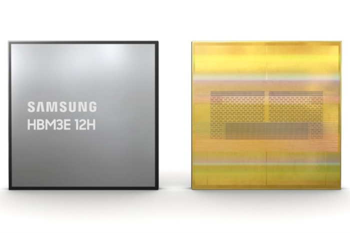
The world’s No. 1 memory chip producer has developed the industry’s biggest 36 GB 12-layer HBM3E
By Feb 27, 2024 (Gmt+09:00)
3
Min read
Most Read
LG Chem to sell water filter business to Glenwood PE for $692 million


KT&G eyes overseas M&A after rejecting activist fund's offer
Kyobo Life poised to buy Japan’s SBI Group-owned savings bank
StockX in merger talks with Naver’s online reseller Kream
Meritz backs half of ex-manager’s $210 mn hedge fund


Samsung Electronics Co. has developed the industry’s first 36-gigabyte (GB) 12-layer high-value, high-performance memory chip in a bid to restore its reputation as a memory giant in the burgeoning high bandwidth memory (HBM) market currently led by its crosstown rival SK Hynix Inc.
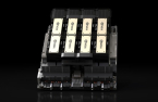
The South Korean chip juggernaut on Tuesday unveiled its fifth-generation HBM product, the HBM3E 12H, which is composed of 12 layers of dynamic random-access memory chips stacked horizontally that boasts the industry’s largest memory capacity of 36 GB for HBM.
The new HBM product’s capacity and performance have improved by more than 50% than its predecessor, the eight-layer HBM3 8H, said the company.
With its most advanced HBM chip, Samsung Electronics is going all out to snatch the crown from its local rival SK Hynix in the HBM market.
The world’s No. 1 memory company said it has already provided HBM3E 12H samples to its customers and plans to mass-produce the chips in the first half of this year.
HBM is a high-value, high-performance memory chip made of vertically interconnected multiple DRAM chips, which significantly speed up data processing compared with general DRAM products, while reducing latency, power and size.
Its demand is rapidly growing as such high-performance chips are essential technology to drive the artificial intelligence revolution.
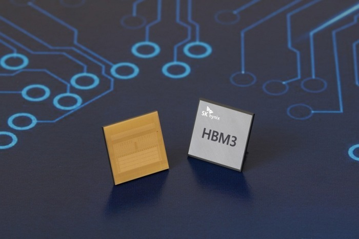
The global HBM market is currently commanded by SK Hynix, the world’s first memory vendor to develop the first-generation HBM chip in 2013 and unveiled succeeding products – the HBM2, HBM2E and the latest and fourth-generation HBM3 chips – in the following years.
It developed the world’s first 12-layer HBM3 with a 24 GB memory capacity in April last year and HBM3E chips four months later.
According to market tracker TrendForce, SK Hynix led the HBM market with a 50% market share as of 2022, followed by Samsung (40%) and Micron Technology Inc. (10%).
SIXTH-GENERATION HBM IN 2026
Samsung Electronics uses advanced thermal compression non-conductive film (TC NCF) to make the height of its newest 12-layer HBM3E product the same as that of the eighth-layer ones.
It also trims the NCF materials' thickness to reduce the gap between chips the industry’s smallest at 7 micrometers (µm), while also eliminating voids between layers, the company said.
During the chip bonding process, the company uses smaller bumps for signaling and larger ones for heat dissipation, which improve the high-performance chip’s production yields.
The HBM3E 12H provides an all-time high bandwidth of up to 1,280 gigabytes per second (GB/s), meaning that with the chip, about 40 UHD movies with a 30GB capacity each can be downloaded per second.
When used in AI applications, it is estimated that the average speed for AI training can be increased by 34% from the HBM3 8H, the company said.
“This new memory solution forms part of our drive toward developing core technologies for high-stack HBM and providing technological leadership for the high-capacity HBM market in the AI era,” Bae Yongcheol, executive vice president of Memory Product Planning at Samsung Electronics, said in a statement.
As the AI chip market is expected to grow tenfold by 2030, Samsung Electronics plans to more than double its HBM capacity this year from last year to lift its HBM output to the industry’s largest.
Its development of the sixth-generation HBM, the HBM4 chip, is also underway to meet the targets to provide its samples in 2025 and mass-produce them in 2026, Samsung Electronics said.
The company is also set to develop a new chip fabrication process to eliminate the gap between chips in the HBM4 16H product line.
Write to Chae-Yeon Kim at why29@hankyung.com
Sookyung Seo edited this article.
More to Read
-
 EarningsSK Hynix swings to profit; sees 60% surge in HBM demand
Jan 25, 2024 (Gmt+09:00)
3 Min read -
 Korean innovators at CES 2024Samsung to double HBM chip production to lead on-device AI chip era
Jan 12, 2024 (Gmt+09:00)
3 Min read -
 Korean chipmakersSamsung, SK pin hopes on HBM sales with Nvidia's new AI chip
Nov 14, 2023 (Gmt+09:00)
2 Min read -
 Korean chipmakersSamsung Elec to launch HBM4 in 2025 to win war in AI sector
Oct 10, 2023 (Gmt+09:00)
2 Min read -
 Korean chipmakersHBM market to nearly double; next-gen DRAM to revive demand: KIW
Sep 11, 2023 (Gmt+09:00)
4 Min read -
 Korean chipmakersSamsung, SK Hynix in next-generation HBM chip supremacy war
Jul 10, 2023 (Gmt+09:00)
3 Min read
Comment 0
LOG IN