Korean chipmakers
Samsung improves 4 nm foundry yields, on par with TSMC: analyst
With its chipmaking tech close to TSMC’s, Samsung now has more chance of bringing fabless customers back into its fold
By Jul 11, 2023 (Gmt+09:00)
4
Min read
Most Read
LG Chem to sell water filter business to Glenwood PE for $692 million


KT&G eyes overseas M&A after rejecting activist fund's offer
Kyobo Life poised to buy Japan’s SBI Group-owned savings bank
StockX in merger talks with Naver’s online reseller Kream
Meritz backs half of ex-manager’s $210 mn hedge fund


Samsung Electronics Co. has improved its chip foundry manufacturing yield for the 4-nanometer node to the level shown by its archrival Taiwan Semiconductor Manufacturing Co. (TSMC), raising its chances of winning back fabless customers, an analyst said.
Park Sang-wook, a semiconductor analyst at HI Investment & Securities, said in a research report on Tuesday that Samsung’s chip production yield rates, the metric that measures the probability of getting good products from manufacturing processes, for the 4 nm and finer 3 nm nodes have improved to over 75% and 60%, respectively.
As recently as early this year, industry officials estimated Samsung’s yield rate for the 4 nm technology to be around 50%.
In advanced processing technology such as 3 nm and 4 nm, a yield rate above 60% means chip production using those processes has reached a stable level.
Currently, 3 nm is the industry’s finest technology with which mass production is possible.
“Samsung’s product launch has been delayed while yield improvement has slowed from the sub-10 nm process, which has led key foundry clients such as Apple, Nvidia and Qualcomm to switch to TSMC,” Park said in the report.
As a result, he said the capital expenditure and production capacity gaps between TSMC and Samsung’s foundry business widened to 3.4 times and 3.3 times, respectively, last year.
“In the processing node below the 7-nanometer technology, TSMC’s market share reached nearly 90% last year, making it harder for Samsung to catch up,” he said.
Samsung is the world’s top memory chipmaker. In the contract manufacturing, or foundry, business, however, it is a distant second with a low double-digit market share after TSMC, which controls more than half the global foundry market.
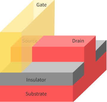
Chipmaking processes carry a numerical label that loosely denotes the size of the transistors that can be packed on a chip. The number refers to the thickness of the circuitry that can be drawn on the transistor. The lower the number, the more advanced the technology.
BETTER CHANCE OF BRINGING CLIENTS BACK TO ITS FOLD
Park, the HI Investment analyst, said now that Samsung’s foundry yields in advanced nodes are nearly on par with TSMC, the chances of the South Korean chipmaker winning clients such as Qualcomm and Nvidia over to its facilities have increased.
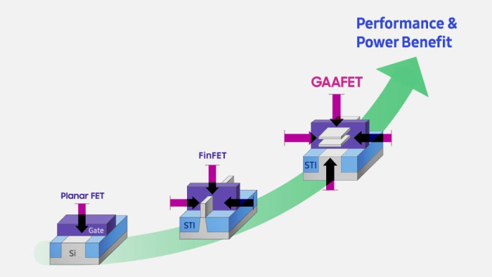
He cited improvements in its 3-5 nm foundry yields, the successful mass production of advanced chips using the next-generation gate-all-around (GAA) technology as the industry’s first to do so, and a sector-wide move to diversify away from TSMC as three factors that boost Samsung’s chances of bringing its former clients back into its fold.
While Samsung’s production tech is based on GAA transistor architecture for its microfabrication process, TSMC uses a different technology in the fin field-effect transistor (FinFET) structure.
The analyst said the current chip industry slowdown has contributed to Samsung improving its manufacturing yields.
“As the fab utilization rate decreased amid an industrywide slowdown, Samsung put in more test wafers to improve its yield rates,” he said.
In the first half, TSMC’s sales revenue reached NT$989 billion, down 3.5% from a year earlier.
BETTER POSITIONED TO COMPETE
With its 3 nm yield rate improved, analysts said Samsung is now better positioned to compete with TSMC in a more advanced 2 nm processing node.
With demand for high-performance chips rising, competition for technology advancement is also fierce, particularly between the two leading foundry players.
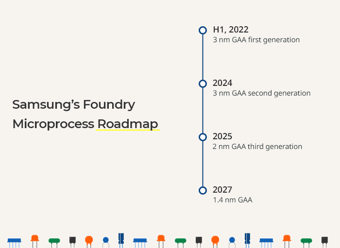
Both companies have vowed to begin mass production of advanced chips using the industry’s cutting-edge 2 nm technology in 2025.
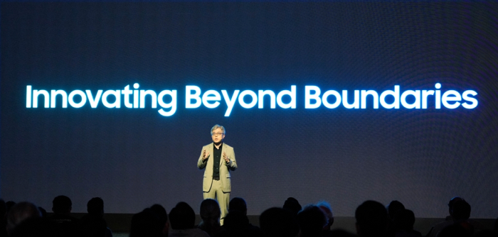
During the late June Samsung Foundry Forum 2023, its annual meeting with clients, Samsung’s foundry business chief Choi Si-young reaffirmed that it will start producing mobile chips in large quantities on its 2 nm node in 2025 as announced earlier.
He said Samsung will apply the 2 nm tech to high-performance computing (HPC) chips for supercomputers and computer clusters in 2026 and then to automotive chips in 2027.
The Samsung executive also said the company plans to begin mass production of more advanced 1.4 nm chips by 2027.
As ultra-fine chipmaking processes pose technological challenges, Samsung said it will use AI and big data technology in its chipmaking process to enhance productivity and refine product quality.
Write to Ik-Hwan Kim at lovepen@hankyung.com
In-Soo Nam edited this article.
More to Read
-
 Korean chipmakersSamsung Electronics to aid foundry clients with state-of-the-art tech
Jul 05, 2023 (Gmt+09:00)
3 Min read -
 Korean chipmakersSamsung’s foundry business to make DDIC chips for LX Semicon
Jul 03, 2023 (Gmt+09:00)
2 Min read -
 Korean chipmakersSamsung on smooth track to 1.4 nm foundry tech to take on TSMC
Jun 28, 2023 (Gmt+09:00)
4 Min read -
 Korean chipmakersIntel’s foundry revamp sets off alarm bells for Samsung, TSMC
Jun 22, 2023 (Gmt+09:00)
4 Min read -
 Korean chipmakersSystem on chips: Samsung’s new high-stakes foundry business
Mar 09, 2023 (Gmt+09:00)
2 Min read -
 Korean chipmakersSamsung Foundry: Driving force behind digital transformation
Dec 01, 2022 (Gmt+09:00)
5 Min read -
 Korean chipmakersShell-First: Samsung Foundry’s custom-tailored new operation strategy
Nov 30, 2022 (Gmt+09:00)
4 Min read -
 Korean chipmakersSamsung sets sights on GAA tech to overtake TSMC in foundry
Nov 29, 2022 (Gmt+09:00)
6 Min read
Comment 0
LOG IN