Semiconductors
Samsung unveils 2.5D chip packaging tech for high-end products
It is suitable for high-performance products that require the integration of multiple chips
By Nov 12, 2021 (Gmt+09:00)
1
Min read
Most Read
LG Chem to sell water filter business to Glenwood PE for $692 million


KT&G eyes overseas M&A after rejecting activist fund's offer
Kyobo Life poised to buy Japan’s SBI Group-owned savings bank
StockX in merger talks with Naver’s online reseller Kream
Meritz backs half of ex-manager’s $210 mn hedge fund


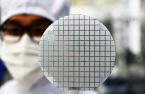
The tech giant said on Thursday its latest 2.5D semiconductor chip packaging technology is now available for clients in artificial intelligence (AI), data center, high-performance computing (HPC) and networking products that require high-performance, large-area packaging.
Samsung Electronics developed the technology in collaboration with Samsung Electro-Mechanics Co. and Amkor Technology Inc., the world’s No. 2 chip packaging company.
With increasing computing power and storage needs, semiconductor chips tend to become larger in size, but Samsung’s H-Cube can fit more in a smaller area and offer compact solutions, it said.
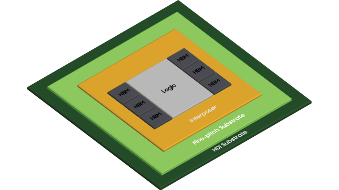
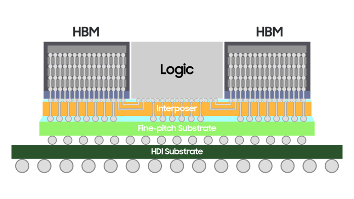
To develop the technology, Samsung said it used a hybrid substrate with a fine-pitch substrate and high-density interconnection (HDI) to fit large sizes into 2.5D packaging.
The packaging allows logic chips or high-bandwidth memory (HBM) to be stacked on top of a silicon interposer in a small form factor, according to Samsung.
It said the technology can fit six HBM chips into a compact area, compared to four under the current packaging technology.
IN COMPETITION WITH TSMC
“By expanding and enriching the foundry ecosystem, we will provide various packaging solutions to find a breakthrough in the challenges our customers face,” said Kang Moonsoo, senior vice president and head of foundry marketing strategy at Samsung.
The announcement comes as Samsung aims to be at the forefront of the packaging industry to gain a fresh edge against Taiwan Semiconductor Manufacturing Co. (TSMC), a major competitor in the ultra-fine processing segment.
Packaging technology can help enhance semiconductor performance without having to shrink the nanometer through ultra-fine processing, which is technologically challenging and requires more time.
Write to Su-Bin Lee at lsb@hankyung.com
In-Soo Nam edited this article.
More to Read
-
 SemiconductorsSamsung overtakes Intel as foundry looms as next battlefield
Aug 02, 2021 (Gmt+09:00)
3 Min read -
 Semiconductor rivalryMemory leader Samsung aims to strengthen system chips, foundry
Jun 08, 2021 (Gmt+09:00)
3 Min read -
 Semiconductor rivalrySamsung loses ground in foundry market as TSMC ties in with Japanese firms
Jun 01, 2021 (Gmt+09:00)
2 Min read -
 Foundry competitionSamsung, TSMC up ante in US foundry competition
May 24, 2021 (Gmt+09:00)
3 Min read -
 Semiconductor shortagesChip shortages spread to backend firms, disrupting supply chains
Feb 15, 2021 (Gmt+09:00)
2 Min read -
 Chip packagingSamsung foundry ramps up chip packaging to compete against TSMC
Nov 30, 2020 (Gmt+09:00)
2 Min read
Comment 0
LOG IN