Korean chipmakers
Samsung's Jay Y. Lee visits Zeiss to reinforce EUV ties
Samsung Electronics is upping the ante to catch up to foundry leader TSMC with the latest EUV lithography technology
By Apr 28, 2024 (Gmt+09:00)
4
Min read
Most Read
Hankook Tire buys $1 bn Hanon Systems stake from Hahn & Co.


NPS to hike risky asset purchases under simplified allocation system
UAE to invest up to $1 bn in S.Korean ventures
Osstem to buy BrazilŌĆÖs No. 3 dental implant maker Implacil
US multifamily market challenges create investment opportunities


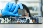
Samsung Electronics Co. is deepening ties with Zeiss Group, the sole provider of optical systems to the worldŌĆÖs only extreme ultraviolet (EUV) lithography system supplier ASML Holding N.V., in next-generation EUV and chip technologies, raising the stakes to overtake the global foundry leader Taiwan Semiconductor Manufacturing Company Ltd. (TSMC).
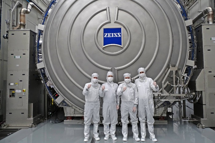
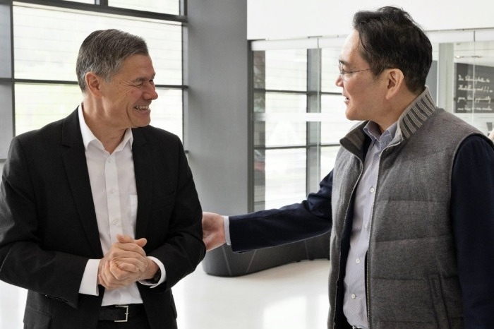
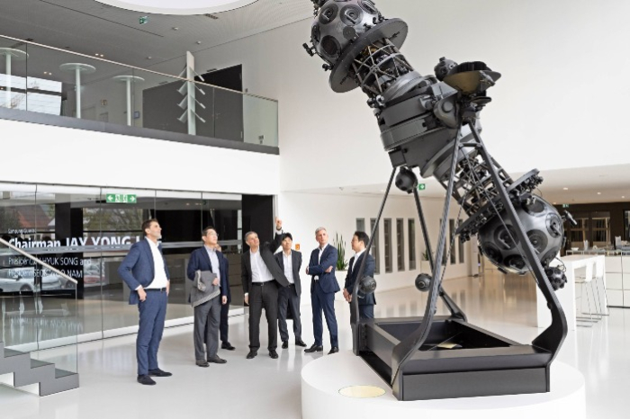
Jay Y. Lee, the executive chairman of the South Korean chip giant, met Karl Lamprecht, president and chief executive officer of Zeiss, and other company executives on Friday during his visit to the headquarters of the global optics and optoelectronics technology conglomerate in Oberkochen, Germany, according to Samsung Electronics on Sunday.
At the meeting, they agreed to expand partnerships in EUV technology and cutting-edge semiconductor equipment research and development to enhance both companies' business competitiveness in the foundry and memory chip sectors.
Samsung Electronics is the worldŌĆÖs top dynamic random-access memory (DRAM) chip producer, and Zeiss is a top multinational optics and optoelectronics solutions developer with over 2,000 core patents in EUV technology, which plays a key role in high-performing advanced chip production.
The German company is also the exclusive supplier of optical products to ASML, the worldŌĆÖs only EUV lithography system provider wielding great power over global chip giants, especially contract chip manufacturers, such as global foundry leader TSMC and distant runner-up Samsung Electronics.
Through deeper ties with Zeiss, the Korean memory giant hopes to improve its next-generation semiconductor technology, optimize its chip fabrication process and refine advanced chip production yields.
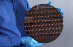
Samsung Electronics aims to lead microfabrication process technology under 3 nanometers, with a plan to mass-produce the sixth-generation 10-nano DRAM chips this year with EUV lithography technology.
EUV AT THE CENTER OF FOUNDRY SUPREMACY
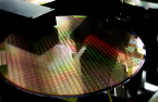
EUV lithography allows chip producers to shrink the size of transistors down to just a few nanometers, tens of thousands of times thinner than a strand of human hair.
The lower the nanometer number, the more advanced the technology, promising a faster computing speed, higher performance and lower power use.
It is considered a crucial technology to developing high-performance chips such as high-bandwidth memory (HBM) chips required to run artificial intelligence-powered devices.

Demand for high-performing memory chips has sharply risen amid the ongoing AI boom. ┬Ā┬Ā
Samsung Electronics is aggressively seeking to commercialize 2nm chips by 2025 and 1.4nm chips by 2027 after mass-producing 3nm chips last year. It became the first foundry company to produce the industryŌĆÖs smallest chip.
Samsung Electronics is the worldŌĆÖs leading memory producer but lags far behind TSMC in the contract chipmaking business. The rivals are in a heated race to lead microfabrication process technology.
The Korean foundry player hopes to leverage more advanced processing technology to overtake its bigger Taiwanese foundry rival.
INVESTMENT FROM ZEISS, ASML
Samsung Electronics has enhanced its partnership with the German optics solution provider in recent years.
In November 2022, Zeiss announced a plan to invest about 48 billion won ($35 million) to build its first-ever foreign country-based R&D center for research microscopy solutions in Korea.
It also plans to open AsiaŌĆÖs first R&D center for its process control solutions for advanced logic and memory chips in the Northeast Asian county.
Zeiss has decided to invest in Korea to meet growing demand for optics solutions not only from the Korean semiconductor sector but also from the battery and electric vehicle industries.
Zeiss also offers photomask solutions, which are essential in the photolithography process. A photomask is an opaque plate or film with transparent areas and a defined pattern.
Its R&D centers in Korea are slated to open in 2026.┬Ā
Lee's visit to Zeiss underscores Samsung Electronics' efforts to build a strong semiconductor supply chain. Its rivals TSMC and Intel are also actively enhancing relationships with leading semiconductor manufacturing equipment providers such as ASML to widen the technology gap with followers.┬Ā
In December last year, Samsung and ASML also signed an agreement to build an EUV R&D facility in Korea with a joint investment of 1 trillion won.
Lee will continue his tour in Europe ŌĆō to France and Italy ŌĆō to check the regional semiconductor supply chain and market, according to Samsung Electronics.┬Ā
Write to Eui-Myung Park at uimyung@hankyung.com
Sookyung Seo edited this article.
More to Read
-
 Korean chipmakersSamsung to unveil Mach-1 AI chip to upend SK HynixŌĆÖs HBM leadership
Mar 20, 2024 (Gmt+09:00)
3 Min read -
 EarningsSamsung Q1 profit soars, set to benefit from Taiwan quake, AI chip demand
Apr 05, 2024 (Gmt+09:00)
3 Min read -
 Korean chipmakersASML, Samsung to build R&D center in Korea for $760 mn
Dec 13, 2023 (Gmt+09:00)
3 Min read -
 Korean chipmakersSamsung to make 2-nanometer GAA chips by 2025 to overtake TSMC
Oct 07, 2021 (Gmt+09:00)
3 Min read -
 Korean chipmakersSamsung, TSMC in heated race for industryŌĆÖs smallest 3 nm process node
Aug 04, 2021 (Gmt+09:00)
4 Min read
Comment 0
LOG IN