Korean chipmakers
ASML, Samsung to build R&D center in Korea for $760 mn
SK Hynix and ASML signed an MOU to jointly develop hydrogen gas recycling technology used for EUV production
By Dec 13, 2023 (Gmt+09:00)
3
Min read
Most Read
LG Chem to sell water filter business to Glenwood PE for $692 million


KT&G eyes overseas M&A after rejecting activist fund's offer
Kyobo Life poised to buy Japan’s SBI Group-owned savings bank
StockX in merger talks with Naver’s online reseller Kream
Meritz backs half of ex-manager’s $210 mn hedge fund


AMSTERDAM, Netherlands -- Samsung Electronics Co. and ASML Holding N.V. have reached a preliminary agreement to build a research and development facility in South Korea with a joint investment of 1 trillion won ($760 million), South Korea’s presidential office said on Wednesday.
Under the memorandum of understanding (MOU) signed at ASML’s headquarters in Veldhoven earlier in the day, the two companies will team up to develop advanced memory chips based on ASML’s latest extreme ultraviolet (EUV) equipment.
ASML is the only EUV scanner maker in the world. The equipment is crucial to draw the most elaborate and detailed patterns on semiconductor wafers, while simplifying the manufacturing process and improving production yields.
“At the R&D center to be established by ASML and Samsung Electronics, they will jointly develop ultra-fine manufacturing processes (for semiconductors) based on (ASML’s) next-generation EUVs,” Park Chun-seop, presidential senior secretary for economic affairs, said in a media briefing.
When completed, the R&D center will mark ASML's first overseas research facility jointly established with a semiconductor company.
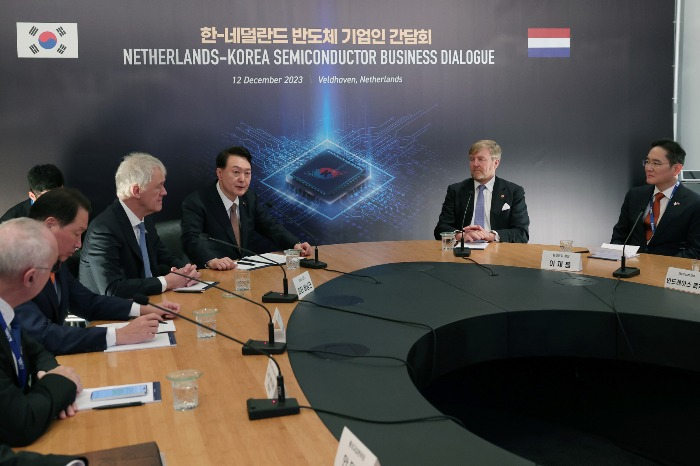
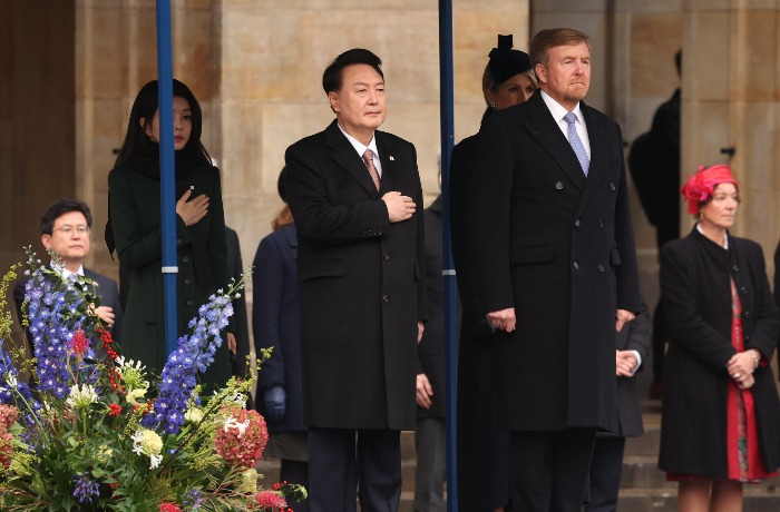
STATE VISIT
The MOU was reached during South Korean President Yoon Suk Yeol’s state visit to the Netherlands this week on the invitation of Willem-Alexander, King of the Netherlands. Yoon and the Dutch king attended the MOU signing ceremony at ASML’s head office.
"The Korean government will strengthen direct communication channels between the two governments and provide all necessary support to ensure the success of this cooperation project," Yoon said in a meeting with chief executives of semiconductor companies from South Korea and the Netherlands.
The presidential senior secretary noted the MOU has great symbolic significance as the first R&D center to be established overseas by ASML and a semiconductor company.
He declined to reveal details such as the ownership ratio of the R&D center and how spending will be split between the two companies.
2-NANOMETER PROCESS
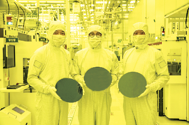
His visit to the country comes as Samsung is making every effort to commercialize 2-nanometer chips by 2025 after mass-producing 3nm chips last year. It became the first foundry company to produce the industry's smallest chip.
ASML has recently developed EUV scanners for the 2nm process or below, which Samsung and its bigger foundry rival TSML are fiercely competing to secure.
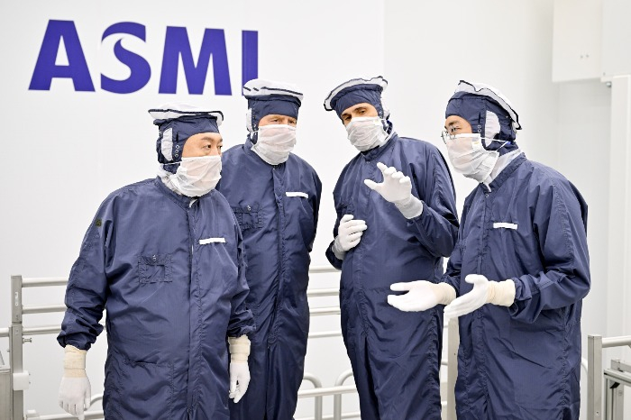
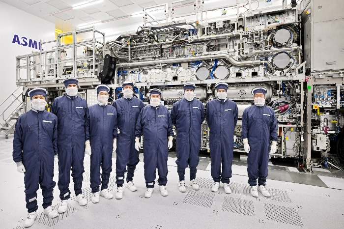
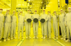
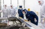
It unveiled the next-generation EUV manufacturing facility to President Yoon. It is the first time for the company to make public the production lines of the 2nm-process EUV machine. He also became the first foreign president to inspect the cleanroom of ASML’s plant.
Jay Y. Lee, chairman of Samsung Electronics Co. and Chey Tae-won, chairman of SK Group, joined Yoon in inspecting ASML’s production lines.
In November of last year, ASML broke ground on a customer education and equipment support service center near Samsung's manufacturing base in Hwaseong, Gyeonggi Province.
For the construction, it plans to invest around 320 billion won. In 1996, it built a customer support center in South Korea.
SK HYNIX-ASML TECHNOLOGY COOPERATION
Separately, SK Hynix Inc., the world’s second-largest memory chipmaker after Samsung, signed an MOU with ASML to jointly develop technology to recycle hydrogen gas used to manufacture EUV machines.
Hydrogen gas recycling is estimated to reduce power consumption per EUV unit by 20% and cut the relevant costs by 16.5 billion won a year.
Apart from the two MOUs signed by Samsung and SK Hynix, South Korea inked an MOU with the Dutch government to make joint efforts to foster semiconductor talent.
Under the preliminary agreement, South Korea’s three graduate schools with departments specializing in semiconductor technology will offer education programs in partnerships with Dutch companies, including ASML, IMEC, Brainport Development, ASM and NXP Semiconductor, as well as Eindhoven University of Technology in the Netherlands.
Yoon became the first South Korean leader to pay a state visit to the Netherlands since the two countries established diplomatic ties in 1961.
Write to Byung-Uk Do at dodo@hankyung.com
Yeonhee Kim edited this article.
More to Read
-
 Korean chipmakersSamsung ‘demanding customer’ for ASML as orders rise
Feb 20, 2023 (Gmt+09:00)
3 Min read -
 Korean chipmakersSamsung to make 3 nm chips for Nvidia, Qualcomm, IBM, Baidu
Nov 22, 2022 (Gmt+09:00)
3 Min read -
 Korean chipmakersSamsung's 3 nm chip narrows microchip gap with TSMC
Jun 30, 2022 (Gmt+09:00)
3 Min read -
 Korean chipmakersSamsung to make 2-nanometer GAA chips by 2025 to overtake TSMC
Oct 07, 2021 (Gmt+09:00)
3 Min read -
 Korean chipmakersASML joins K-Semiconductor Belt with $210 mn investment by 2025
May 13, 2021 (Gmt+09:00)
2 Min read
Comment 0
LOG IN