Korean chipmakers
Samsung, Arm reinforce alliance on future AI chips
The South Korean chip giant has optimized Arm’s newest CPU model Cortex-X on its latest GAA process
By Feb 21, 2024 (Gmt+09:00)
4
Min read
Most Read
LG Chem to sell water filter business to Glenwood PE for $692 million


KT&G eyes overseas M&A after rejecting activist fund's offer
Kyobo Life poised to buy Japan’s SBI Group-owned savings bank
StockX in merger talks with Naver’s online reseller Kream
Meritz backs half of ex-manager’s $210 mn hedge fund


Samsung Electronics Co. will offer Arm Inc.’s most advanced central processing unit (CPU) optimized on its latest gate-all-around (GAA) technology, a move expected to accelerate a new class of system on chips (SoCs) with generative artificial intelligence capabilities.
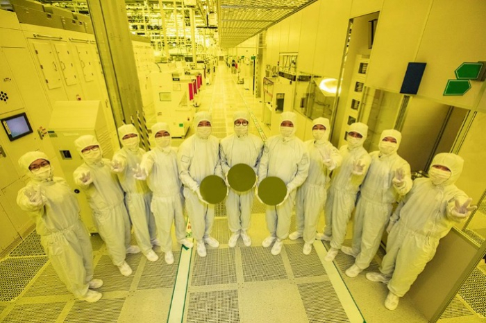
The South Korean chip giant announced on Wednesday it has optimized the British semiconductor design firm's latest Cortex-X CPU with its 3-nanometer GAA processing technology, preparing to offer it to fabless chipmakers.
With the latest development, Samsung’s foundry customers will be able to use Arm’s most advanced CPU in developing their SoCs designed to bolster AI computing, a move that's expected to lure more fabless chipmakers to join Samsung Foundry, Samsung’s foundry business, as customers.
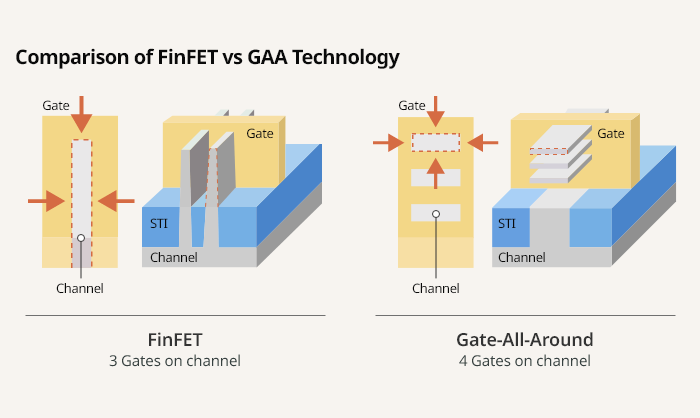
GAA is Samsung’s latest chip processing technology designed to ensure maximum design flexibility and scalability for better power efficiency and chip performance than those produced by the fin field-effect transistor (FinFET) process. It is considered a game changer in the semiconductor sector.
The Korean chip giant was the world’s first to implement the 3 nm GAA processing technology, in June 2022, and is now developing the second-generation 3 nm GAA node as well as the 2 nm GAA architecture.

Arm’s Cortex-X CPU is regarded as its most advanced chip architecture that can be used in servers and data centers in addition to mobile devices.
SoC is an all-in-one semiconductor composed of several devices such as a CPU, a memory system like dynamic random-access memory (DRAM), a digital signal processor, a graphics processing unit and other central semiconductor elements.
Following their latest collaboration, Samsung and Arm plan to reinvent 2 nm GAA for next-generation data centers and infrastructure custom silicon, as well as an AI chiplet for the next-generative AI mobile computing market, according to Samsung.
Samsung posted $16 billion in foundry orders in 2023, its highest-ever annual result, said Kim Dong-won, an analyst at KB Securities Co., adding he expects the company’s foundry customers to jump to 210 in 2028 from 120 in 2023.
London-based tech research group Omdia also forecast the global foundry market to grow at a compound annual growth rate of 13.8% from 2023 to 2026. In particular, the market for 3-nanometer and smaller nodes is expected to grow at a 64.8% CAGR over the same period.
GAA AS A GAME CHANGER
GAA, also called multi-bridge-channel FET (MBCFET), defies the performance limits of FinFET. It improves power efficiency by reducing the supply voltage level while enhancing performance by increasing drive current capability, the company said.
With demand for high-performance computing (HPC) chips used in supercomputers and computer clusters growing, competition to advance technology is fierce.
Samsung and its larger foundry rival Taiwan Semiconductor Manufacturing Company Ltd. (TSMC) are keen to employ the 3 nm process node, the industry’s narrowest circuitry, to manufacture chips with increased transistor density, faster data speed and reduced power consumption.
Nano refers to the width of the chip circuit line. The thinner the circuit linewidth, the higher the chip performance and energy efficiency because a larger number of chips can be mounted on a substrate or wafer.
While Samsung is considered the GAA pioneer, TSMC opts for the FinFET node.
Designed with Samsung’s 3 nm GAA process node, Arm’s Cortex-X CPUs' performance and efficiency have improved, taking the user experience to the next level, Samsung said.

This is not the first collaboration between the two companies. They have been working together for more than a decade, including their partnership on 7 nm and 5 nm FinFET processing nodes announced in July 2018.
The long-time allies expect their latest partnership to play a vital role in enabling next-generation chip innovations for the AI era.
“As we continue into the Gen AI era, we are excited to extend our partnership with Arm to deliver the next generation Cortex-X CPU, enabling our mutual customers to create innovative products,” said Kye Jongwook, executive vice president and head of Foundry Design Platform Development at Samsung Electronics.
“Optimizing Cortex-X and Cortex-A processors on the latest Samsung process node underscores our shared vision to redefine what’s possible in mobile computing, and we look forward to continuing to push boundaries to meet the relentless performance and efficiency demands of the AI era,” said Chris Bergey, senior vice president of Client Business at Arm Inc.
Write to Chae-Yeon Kim at why29@hankyung.com
Sookyung Seo edited this article.
More to Read
-
 Korean chipmakersSamsung sets sights on GAA tech to overtake TSMC in foundry
Nov 29, 2022 (Gmt+09:00)
6 Min read -
 Korean chipmakersSamsung to make 3 nm chips for Nvidia, Qualcomm, IBM, Baidu
Nov 22, 2022 (Gmt+09:00)
3 Min read -
 Korean chipmakersSoftBank’s Son expected to meet Samsung's Lee for Arm M&A discussion
Oct 02, 2022 (Gmt+09:00)
5 Min read -
 Korean chipmakersSamsung nears 3-nano chip mass production ahead of TSMC
Jun 28, 2022 (Gmt+09:00)
3 Min read -
 Korean chipmakersSamsung, TSMC in heated race for industry’s smallest 3 nm process node
Aug 04, 2021 (Gmt+09:00)
4 Min read
Comment 0
LOG IN