Korean chipmakers
SK Hynix unveils another NAND to win chip stacking war
The world’s No. 2 memory chipmaker introduces the industry’s first 321-layer NAND with 59% productivity improvement
By Aug 09, 2023 (Gmt+09:00)
2
Min read
Most Read
LG Chem to sell water filter business to Glenwood PE for $692 million


KT&G eyes overseas M&A after rejecting activist fund's offer
Kyobo Life poised to buy Japan’s SBI Group-owned savings bank
StockX in merger talks with Naver’s online reseller Kream
Meritz backs half of ex-manager’s $210 mn hedge fund


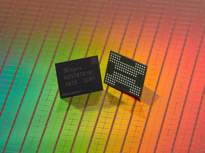
SK Hynix Inc., the world’s second-largest memory chipmaker after Samsung Electronics Co., showcased its progress in the chip stacking technology race to meet increasing demand for high-performance and high-capacity products amid the rapid growth in artificial intelligence by unveiling the industry’s first NAND chips with more than 300 layers.
SK Hynix said on Wednesday that it introduced a sample of the 321-layer four-dimensional (4D) NAND at the Flash Memory Summit in Santa Clara, California. The South Korean tech giant plans to start mass production of the 1-terabit (Tb) triple-level cell (TLC) 4D NAND flash in the first half of 2025.
“With timely introduction of the high-performance and high-capacity NAND, we will strive to meet the requirements of the AI era and continue to lead innovation,” said Choi Jungdal, SK Hynix’s head of NAND development, during a keynote speech at the conference.
Demand for advanced memory chips that can process more data at a faster pace has been increasing with the rapid growth in generative AI applications such as ChatGPT developed by Microsoft Corp.-backed OpenAI.
IMPROVES PRODUCTIVITY BY 59%
SK Hynix said the 321-layer NAND has improved productivity by 59% compared with its 238-layer, 512 Gb 4D NAND chips, the industry’s highest-layered and smallest NAND chips available so far. The company began mass production of the product in May.
The company said its technological competitiveness accumulated from the 238-layer NAND helped make progress for the development of the 321-layer product.
“With another breakthrough to address stacking limitations, SK Hynix will open the era of NAND with more than 300 layers and lead the market,” the company said in a statement.
It also introduced next-generation NAND solutions optimized for such AI demand, including the enterprise solid-state drive (SSD) adopting the fifth-generation PCIe interface and UFS 4.0 at the conference.
PCIe, short for peripheral component interconnect express, is a serial-structured high-speed input and output interface used in the main boards of digital devices. UFS stands for universal flash storage, a flash storage specification for digital cameras, mobile phones and other consumer electronics.
SK Hynix said that it has begun development of the sixth-generation PCIe and UFS 5.0 with improved technology for solution development acquired through the PCIe Gen5 and UFS 4.0.
Write to Jeong-Soo Hwang at hjs@hankyung.com
Jongwoo Cheon edited this article.
More to Read
-
 Korean chipmakersSK Hynix steps up chip stacking war with 238-layer 4D NAND
Jun 08, 2023 (Gmt+09:00)
3 Min read -
 Korean chipmakersSK Hynix unveils world's first 238-layer NAND; Samsung SSD 20 times faster
Aug 03, 2022 (Gmt+09:00)
3 Min read -
 Korean chipmakersAI-driven GPU, advanced chip shortage: Boon for Samsung, SK Hynix
May 31, 2023 (Gmt+09:00)
3 Min read
Comment 0
LOG IN