Korean chipmakers
Samsung eyes wider foundry client base with Ambarella deal
The Korean tech giant aims to raise the number of its foundry clients fivefold by 2027 with advanced 5 nm and 4 nm nodes
By Feb 21, 2023 (Gmt+09:00)
2
Min read
Most Read
LG Chem to sell water filter business to Glenwood PE for $692 million


KT&G eyes overseas M&A after rejecting activist fund's offer
Kyobo Life poised to buy Japan’s SBI Group-owned savings bank
StockX in merger talks with Naver’s online reseller Kream
Meritz backs half of ex-manager’s $210 mn hedge fund


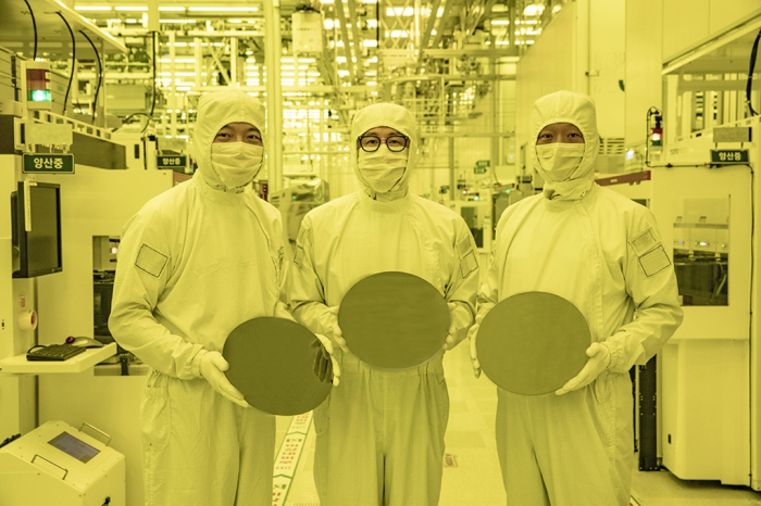
Samsung Electronics Co., the world’s largest memory chipmaker, said on Tuesday it will manufacture automotive chips for US chip designer Ambarella Inc. with its advanced 5-nanometer processing technology.
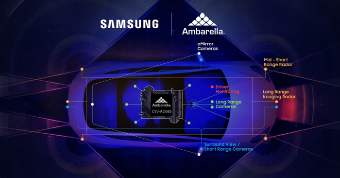
Under the deal, Samsung Foundry, the South Korean chipmaker’s contract chipmaking unit, will produce the Santa Clara-based company’s automotive AI central domain controller, the CV3-AD685.
The CV3-AD685, the US fabless firm’s latest system-on-chip (SoC), is used in the advanced driver assistance system (ADAS), one of the key devices for self-driving cars.
“This collaboration will improve the autonomous driving vehicle safety by taking AI performance, power and reliability to the next level,” Samsung said in a statement.
Ambarella said the latest chip integrates its next-generation CVflow AI engine, which includes neural network processing that is 20 times faster than its previous model.
“Ambarella and Samsung Foundry have a rich history of collaboration. We’re excited to bring Samsung’s world-class 5 nm technology to our new SoCs,” said Ambarella Chief Executive Fermi Wang.
The CV3-AD685 chip will process data for autonomous driving from Level 2 to Level 4, the companies said.
Ambarella’s products are used in a variety of edge AI applications, including ADAS, video security and robotics.
TO WIDEN FOUNDRY CLIENT BASE
Samsung, the world’s second-largest foundry player after industry leader Taiwan Semiconductor Manufacturing Co. (TSMC), is striving to widen its foundry client base, from traditional fabless companies, including Qualcomm Technologies and Nvidia, to Big Tech such as Google, Microsoft and Tesla, which want to make their own chips.
Recently, Samsung said it began utilizing more advanced 4 nm technology to make automotive chips for its clients.
The company said in December that its foundry business revenue exceeded that of its mainstay NAND flash chips – an indication that the Korean tech giant is gaining traction in its bid for a greater role in the contract chip manufacturing segment.
Samsung aims to raise the number of its foundry clients fivefold by 2027 compared to 2019.
To achieve that goal, it said it will diversify its business portfolio by ensuring that non-mobile applications such as high-performance computing (HPC), 5G connectivity and automotive chips account for more than half of its foundry sales by 2027.
According to market research firm Omdia, the global foundry market, expected to reach $125.2 billion by year-end, is forecast to grow at an annual average rate of 10.3% over the next five years.
Samsung said it plans to significantly increase its foundry capacity at its main Pyeongtack plant this year and begin operations at its Taylor, Texas plant by the end of 2024 to triple the company’s 2022 global contract chipmaking capacity by 2027.
Write to Sungsu Bae at baebae@hankyung.com
In-Soo Nam edited this article.
More to Read
-
 Korean chipmakersSamsung’s foundry revenue exceeds mainstay NAND chip sales
Dec 13, 2022 (Gmt+09:00)
3 Min read -
 Korean chipmakersSamsung Foundry: Driving force behind digital transformation
Dec 01, 2022 (Gmt+09:00)
5 Min read -
 Korean chipmakersShell-First: Samsung Foundry’s custom-tailored new operation strategy
Nov 30, 2022 (Gmt+09:00)
4 Min read -
 Korean chipmakersSamsung sets sights on GAA tech to overtake TSMC in foundry
Nov 29, 2022 (Gmt+09:00)
6 Min read -
 Korean chipmakersSamsung mulls new foundry plant in Europe, to expand outsourcing
Oct 19, 2022 (Gmt+09:00)
3 Min read
Comment 0
LOG IN