Korean chipmakers
Samsung unveils industry’s first 12 nm DRAM, compatible with AMD
At its two-day strategy meeting this week, Samsung plans to discuss foundry, AI and automotive chips
By Dec 21, 2022 (Gmt+09:00)
2
Min read
Most Read
LG Chem to sell water filter business to Glenwood PE for $692 million


KT&G eyes overseas M&A after rejecting activist fund's offer
Kyobo Life poised to buy Japan’s SBI Group-owned savings bank
StockX in merger talks with Naver’s online reseller Kream
Meritz backs half of ex-manager’s $210 mn hedge fund


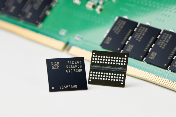
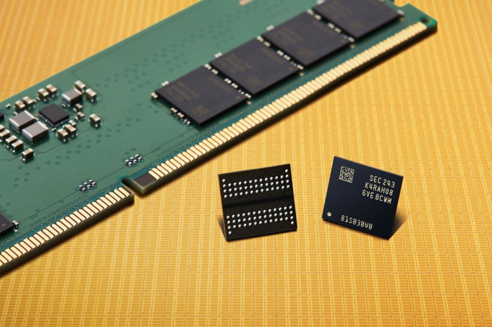
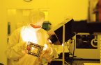
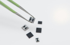
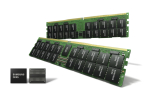
Samsung Electronics Co., the world’s largest memory chipmaker, said on Wednesday it has unveiled an advanced DRAM chip, using the industry’s finest 12-nanometer process node, further widening its lead over rivals in chip processing technology.
The next-generation double data rate 5 (DDR5) chip made with the 12 nm tech – the industry’s first to do so – boasts a data transfer rate of up to 7.2 gigabits per second (Gbps). At this speed, the hardware can transmit two 30 gigabyte (GB) ultra-high-definition movies in a second, the company said.
The South Korean tech giant said the 12 nm process technology improves power efficiency by consuming 23% less power than the previous DRAM model.
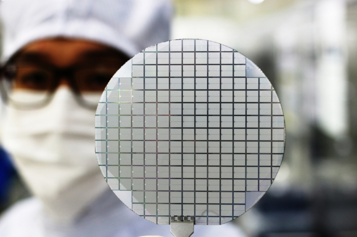
In the chipmaking process, nanometer refers to the circuitry size of the transistors that can be packed on a chip. The lower the nanometer number, the more advanced the technology, promising a faster computing speed, higher performance and lower power use.
Samsung said it also proved the performance of its 16-gigabit DDR5 DRAM built with the 12 nm-class process tech through a compatibility test with CPU maker Advanced Micro Devices Co.
“We are thrilled to once again collaborate with Samsung, particularly on introducing DDR5 memory products that are optimized and validated on Zen platforms,” said Joe Macri, senior vice president and chief technology officer at AMD.
“Innovation often requires close collaboration with industry partners to push the bounds of technology.”
DRAM makers, including Micron Technology Inc. and SK Hynix Inc., are largely using a 14 nm node to produce DDR5 DRAM chips.
In October 2021, Samsung said it successfully produced a 14 nm DDR5 chip, applying extreme ultraviolet (EUV) technology.
The company said on Wednesday its latest 12 nm DDR5 chip also uses EUV tech to improve productivity by 20%.
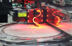
EUV is a chip fabricating technology that reduces the steps in multi-patterning and improves patterning accuracy on wafers, ensuring better semiconductor performance, greater yields, and a shorter chip development time.
MASS PRODUCTION IN 2023
Samsung plans to begin mass production of the 12 nm DDR5 DRAM in 2023, targeting high-performance computing (HPC), data centers and artificial intelligence (AI) applications.
“Our 12 nm-range DRAM will be a key enabler in driving market-wide adoption of DDR5 DRAM,” said Lee Joo-young, executive vice president and head of DRAM product & technology at Samsung.
The company said it will broaden its DRAM lineup built on the cutting-edge 12 nm-class process technology as it continues to work with industry partners to support the rapid expansion of next-generation computing.
Meanwhile, Samsung said its Device Solutions (DS) division, which is in charge of the semiconductor business, will hold a two-day strategy meeting from Thursday.
At the biannual meeting, Samsung executives will discuss ways to improve the foundry business' competitiveness and expand investment in the AI and automotive chip businesses, a company official said.
Write to Jeong-Soo Hwang at hjs@hankyung.com
In-Soo Nam edited this article.
More to Read
-
 Korean chipmakersSamsung Foundry: Driving force behind digital transformation
Dec 01, 2022 (Gmt+09:00)
5 Min read -
 Korean chipmakersShell-First: Samsung Foundry’s custom-tailored new operation strategy
Nov 30, 2022 (Gmt+09:00)
4 Min read -
 Korean chipmakersSamsung sets sights on GAA tech to overtake TSMC in foundry
Nov 29, 2022 (Gmt+09:00)
6 Min read -
 Korean chipmakersSamsung, Qualcomm unveil industry’s fastest LPDDR5X DRAM chip
Oct 18, 2022 (Gmt+09:00)
1 Min read -
 Korean chipmakersMicron’s entry into DDR5 market: A boon for Samsung, SK Hynix
Aug 30, 2022 (Gmt+09:00)
2 Min read -
 Korean chipmakersSamsung makes industry’s smallest 14 nm DDR5 chip with EUV technology
Oct 12, 2021 (Gmt+09:00)
4 Min read
Comment 0
LOG IN