Samsung sets up team to win AI chip deal from Nvidia
Samsung gears up to take on HBM leader SH Hynix with its 12-layer HBM3E, which may be used for NvidiaŌĆÖs new products
By May 06, 2024 (Gmt+09:00)
Deutsche Bank's Korea IB head quits after country head resigns


Macquarie Korea Asset Management confirms two nominees


Hanwha buys SŌĆÖpore Dyna-MacŌĆÖs stake for $73.8 mn from Keppel


Korea's Taeyoung to sell local hotel to speed up debt workout


Meritz leaves door open for an M&A, to stay shareholder friendly


Samsung Electronics Co., the worldŌĆÖs top memory chipmaker, established a team for a billions-of-dollars high-bandwidth memory chip supply deal with Nvidia Corp., the global artificial intelligence semiconductor giant, to beat the HBM market leader SK Hynix Inc.
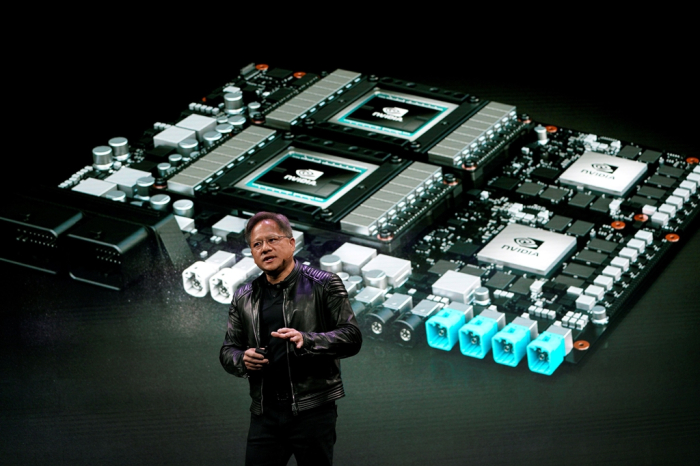
The task force with about 100 excellent engineers has been working to improve manufacturing yields and quality with their first aim to pass NvidiaŌĆÖs tests as Nvidia CEO Jensen Huang asked the South Korean company to raise the yields and quality of both 8-layer and 12-layer HBM3E chips for supply, according to industry sources in Seoul on Monday. HBM3E is the industryŌĆÖs best-performing DRAM chip for AI applications.
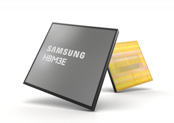
Samsung is focusing on the worldŌĆÖs first 36-gigabyte (GB) 12-layer HBM3E model it developed in February with hopes to pass the quality test currently conducted by Nvidia this month. Samsung has reportedly secured production lines already to increase output to meet NvidiaŌĆÖs demand, sources said. The 12-layer HBM3E improves AI learning speed by 34% on average compared to the 8-layer product.
ŌĆ£Samsung aims to log a high market share by quickly increasing supply to Nvidia,ŌĆØ said one of the sources. ŌĆ£It is expected to speed up the supply from the third quarter.ŌĆØ
The strategy came as SK Hynix Inc., the worldŌĆÖs No. 2 memory chipmaker, dominates the global HBM market with a market share of more than 90%.
ŌĆ£We lost the first battle but have to win the second,ŌĆØ said Samsung President & CEO Kyung Kye Hyun, who manages the tech giantŌĆÖs chip businesses.
GROWING COMPETITION
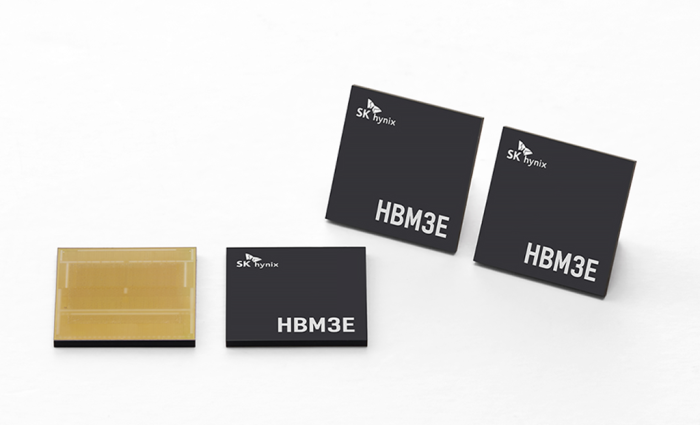
SK Hynix, which has already been selling 8-layer HBM3E to Nvidia, also provided 12-layer product samples to the US graphics chip designer for performance evaluation for supply from the third quarter.
ŌĆ£It is impossible to secure a competitive edge in an instant,ŌĆØ said SK Hynix Chief Executive Kwak Noh-jung. ŌĆ£But we wonŌĆÖt be complacent.ŌĆØ

It was the first time for Samsung and SK Hynix were competing to supply a single client -- Nvidia, the worldŌĆÖs only HBM3E customer -- with the same product at the same time. Nvidia is expected to place orders worth more than 10 trillion won ($7.3 billion) this year.
The two South Korean rivals are likely to win the deals but their supply volumes will be different, industry sources said.
TAILORED PRODUCT
HBM, a high-performance memory chip stacking multiple DRAMs vertically manufactured with the through silicon via (TSV) process, is an essential component of AI chips in processing great volumes of data.
HBM is optimized for a graphics processing unit (GPU), a brain for an AI accelerator ŌĆō a class of specialized hardware accelerator or computer system designed to speed up AI and machine learning applications ŌĆō as its bandwidth and storage capacity are more than 10 times larger than ordinary chips.
The next-generation chips are tailored for customers as their manufacturing requires advanced technology.
Its growing popularity changed the landscape of the memory chip industry, which had been concentrating on general-purpose products.
SLUGGISH START
The global memory chip industry started developing HBM since graphics card makers for games such as Nvidia and Advanced Micro Devices Inc. (AMD) asked to produce DRAM chips with high bandwidth in 2010. Those clients needed to make graphics cards, which could process large amounts of pixel data to handle high-definition games, at a time when the performance of DRAM for GPUs was weak.
SK Hynix joined hands with AMD to research and unveiled an HBM at the International Solid-State Circuits Conference in February 2013.
In June 2015, AMD CEO Lisa Su introduced another HBM at a game event. Its performance was not strong enough to offset high production expenses, however. The price of the HBM was nearly triple that of the graphics double data rate (GDDR) as the 2.5D packaging methodology was applied to the TSV process to connect GPU and HBM. That caused the US fabless chip designer to give up adding HBM to graphics cards.
Nvidia decided to install HBM on servers as the product was suitable for processing large amounts of data, however. The dominant AI accelerator maker with a market share of 97.2% in 2023 equipped HBM2 to its Tesla P100 data center accelerator in 2016.
The move did not expand the HBM market, which accounted for only 5% of the total global DRAM sales, as demand for AI accelerators remained weak.
PAID OFF WITH AI
The HBM market has been significantly growing since generative AI such as ChatGPT emerged in 2022, which prompted global Big Tech companies to rush for investments in the sector.
SK Hynix was the major beneficiary as the company was the only chipmaker that could manufacture HBM3, the fourth-generation product with a bandwidth of 819 GB per second, 6.4 times the first-generation HBMŌĆÖs 128 GB. The South Korean company made up more than 90% of the global HBM3 market, while Samsung failed to share the boom as it stopped developing HBM in 2019.
The prices of HBM3 are reportedly more than five times those of ordinary DRAMs and their profit margins are around 50%.
Thanks to the next-generation products, SK Hynix reported an operating profit of 2.9 trillion won in the first quarter, far more than SamsungŌĆÖs 1.9 trillion won.
The Suwon, South Korea-based company has recently started mass production of HBM3, but it won't be easy to break the relationship between Nvidia and SK Hynix in the near term.
NVIDIA ASKS TO SPEED UP SUPPLIES
Samsung geared up to take on SK Hynix with its 12-layer HBM3E, which is likely to be used for NvidiaŌĆÖs next-generation AI accelerators such as the B200 and GB200.
The B200 needs eight 8-layer HBM3Es, compared to the previous H100 and H200, which are equipped with four HBM3s and six HBM3s, respectively. The upgraded versions of B200 and GB200 are predicted to require more than eight 12-layer HBM3Es.
That is expected to nearly quadruple to $16.9 billion this year from $4.4 billion in 2023. The market is likely to grow further by 2030.

Nvidia CEO Huang has reportedly asked both Samsung and SK Hynix to speed up supplies, intensifying their competition.
That could provide Samsung with chances to beat SK Hynix in the HBM market but also allows SK Hynix the opportunity to maintain the throne, industry sources said.
Write to Jeong-Soo Hwang at hjs@hankyung.com
┬Ā
Jongwoo Cheon edited this article.
-
 Korean chipmakersSK HynixŌĆÖs HBM chip orders fully booked; 12-layer HBM3E in Q3: CEO
May 02, 2024 (Gmt+09:00)
5 Min read -
 EarningsSK Hynix, latest chipmaker to emerge victorious with record Q1 sales
Apr 25, 2024 (Gmt+09:00)
3 Min read -
 Korean chipmakersSamsung shifts gears to focus on HBM, server memory chips
Apr 30, 2024 (Gmt+09:00)
3 Min read -
 Korean chipmakersSK Hynix to invest $14.6 bn to build HBM plant in S.Korea
Apr 24, 2024 (Gmt+09:00)
4 Min read -
 Korean chipmakersSK Hynix, TSMC tie up to stay ahead of Samsung for HBM supremacy
Apr 19, 2024 (Gmt+09:00)
4 Min read -
 Korean chipmakersSamsung establishes HBM team to up AI chip production yields
Mar 29, 2024 (Gmt+09:00)
2 Min read -
 Korean chipmakersSamsung set to triple HBM output in 2024 to lead AI chip era
Mar 27, 2024 (Gmt+09:00)
3 Min read -
 Korean chipmakersSamsung rallies on expectations of NvidiaŌĆÖs HBM order
Mar 20, 2024 (Gmt+09:00)
3 Min read -
 Korean chipmakersSK Hynix mass-produces HBM3E chip to supply Nvidia
Mar 19, 2024 (Gmt+09:00)
3 Min read -
 Korean chipmakersSamsung doubles down in HBM race with largest memory
Feb 27, 2024 (Gmt+09:00)
3 Min read


