Korean chipmakers
Samsung to relocate packaging unit workplace to lure talent
Samsung, SK Hynix absorb advanced packaging engineers to expand the business; OSAT firms suffer talent turnover
By Dec 14, 2023 (Gmt+09:00)
3
Min read
Most Read
LG Chem to sell water filter business to Glenwood PE for $692 million


KT&G eyes overseas M&A after rejecting activist fund's offer
Kyobo Life poised to buy Japan’s SBI Group-owned savings bank
StockX in merger talks with Naver’s online reseller Kream
Meritz backs half of ex-manager’s $210 mn hedge fund


Samsung Electronics Co., the world’s top memory chipmaker, is set to relocate its advanced packaging department’s workplace in South Korea to retain employees at and attract talent to the priorized unit amid the boom in artificial intelligence.
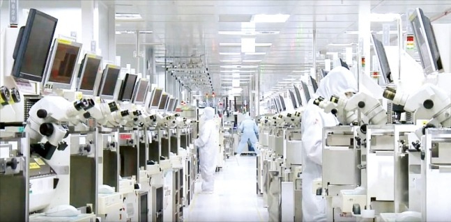
Samsung is seeking to move the workplace of the department’s development team in the country to Yongin or Hwaseong, both about 50 kilometers (31 miles) south of Seoul from the current Cheonan, about 100 km south of the capital, according to industry sources on Wednesday. The company manufactures semiconductors in Yongin and Hwaseong while operating chip production lines with advanced packaging technology in Cheonan.
The plan came as packaging engineers have been reluctant to join Samsung as the present workplace is far from Seoul. Recruitment to the unit has been difficult even though it is only about a one-hour commute to Seoul by bullet train.
“Samsung is aiming to prevent the existing employees from leaving and attract external talent by relocating the workplace to the center of Gyeonggi Province, the Maginot Line for commuting to and from the Seoul metropolitan area,” said one of the sources.
RAPID GROWTH
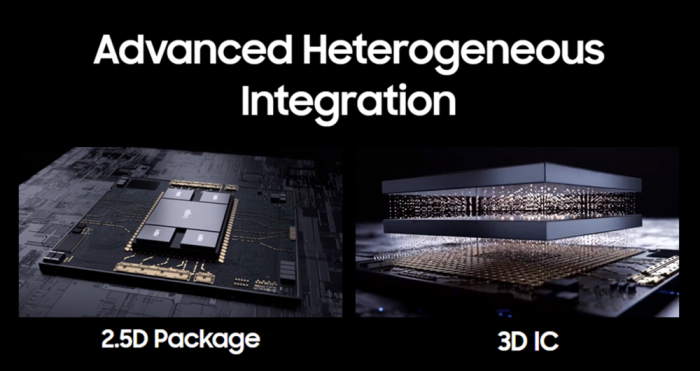
The company and its smaller rival SK Hynix Inc. have been scrambling for advanced packaging engineers. Advanced packaging integrates different semiconductors or vertically interconnects multiple chips. It also allows multiple devices to be merged and packaged as a single electronic device.
Need for the technology has been surging in line with growth in generative AI such as ChatGPT, a chatbot developed by Microsoft Corp.-backed OpenAI, which requires semiconductors with large data processing capacity.
The global semiconductor industry is struggling to improve chip performance with ultra-fine processes. The costs to develop new technology, however, has ballooned as the industry started producing chips with node sizes 3 nanometers or smaller.
Chipmakers and their customers pay attention to advanced packaging technologies that increase performance through efficient arrangement of existing semiconductors.
The global advanced packaging market was forecast to swell by 77.4% to $78.6 billion by 2028 from $44.3 billion in 2022, according to industry consulting firm Yole Intelligence.
TALENT WAR
Samsung established the advanced packaging business department in December 2022 under the direct control of Kyung Kye Hyun, president and CEO of Samsung’s device solution division that handles the global operations of the memory, system LSI and foundry business units.
In March, the company appointed Lin Jun-cheng, a veteran engineer of the global foundry leader Taiwan Semiconductor Manufacturing Co.’s (TSMC) advanced packaging and testing department, as a vice president of the business.
Samsung recruited advanced packaging experts from the group’s information technology affiliates such as Samsung Display Co. to quickly acquire qualified talent, industry sources said.
“We have no choice as the department is strategically nurtured by the big brother Samsung Electronics,” said an official at one of the affiliates.
SK Hynix is expanding the advanced packaging business by personnel transfer and has increased the number of its executives by 25% in a year. The world’s second-largest memory chipmaker is also operating an in-house career development program to foster talent.
Such moves have led to a rise in employee turnovers at outsourced semiconductor assembly and test (OSAT) companies such as Amkor Technology Inc. and STATS ChipPAC Ltd.
“We are facing a crisis in staff management as more and more engineers with three to four years of experience we painstakingly nurtured left for major chipmakers such as Samsung Electronics and SK Hynix,” said an official at an OSAT company.
Write to Jeong-Soo Hwang, Ik-Hwan Kim and Ye-Rin Choi at hjs@hankyung.com
Jongwoo Cheon edited this article.
More to Read
-
 Korean chipmakersSamsung set to supply HBM3, packaging services to AMD
Aug 22, 2023 (Gmt+09:00)
1 Min read -
 Korean chipmakersSamsung Elec to provide HBM3, packaging service to Nvidia
Aug 01, 2023 (Gmt+09:00)
5 Min read -
 Korean chipmakersS.Korea's chip pioneer Amkor aims to rule packaging sector
Jun 18, 2023 (Gmt+09:00)
4 Min read -
 Korean chipmakersSamsung Elec launches foundry package turnkey service
Apr 14, 2023 (Gmt+09:00)
3 Min read -
 Corporate investmentSK to build first chip packaging plant in US with $22 bn investment
Jul 27, 2022 (Gmt+09:00)
4 Min read
Comment 0
LOG IN