Korean chipmakers
Samsung to apply AI, big data tech to entire chipmaking process
Wider use of AI in the chip manufacturing process will also help Samsung catch up to bigger rival TSMC, analysts say
By Jun 19, 2023 (Gmt+09:00)
3
Min read
Most Read
LG Chem to sell water filter business to Glenwood PE for $692 million


KT&G eyes overseas M&A after rejecting activist fund's offer
Kyobo Life poised to buy Japan’s SBI Group-owned savings bank
StockX in merger talks with Naver’s online reseller Kream
Meritz backs half of ex-manager’s $210 mn hedge fund


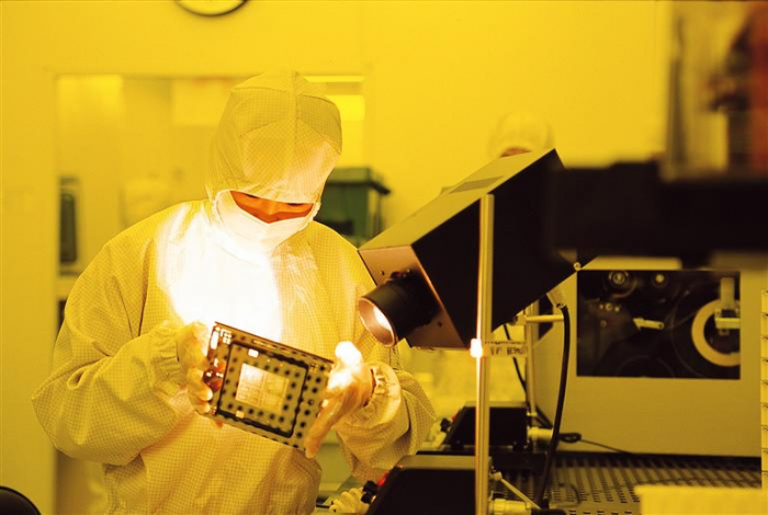
Samsung Electronics Co., the world’s largest memory chipmaker, plans to use AI and big data technology in its chipmaking process to enhance productivity and refine product quality.
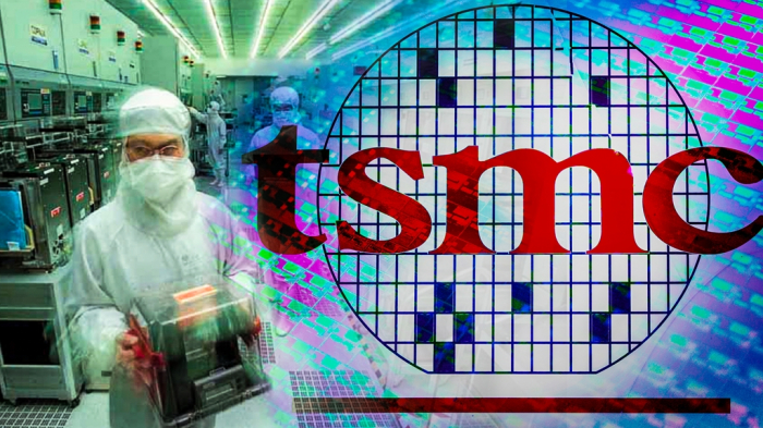
The move, to be led by Kyung Kye-hyun, president and head of Samsung’s semiconductor business, is also aimed at catching up to bigger foundry rival Taiwan Semiconductor Manufacturing Co. (TSMC) by improving manufacturing yields on wafers.
In partnership with the Samsung Advanced Institute of Technology (SAIT), Samsung’s Device Solutions (DS) division, which oversees its semiconductor business, will lead the company’s efforts to broaden the use of AI throughout the chipmaking process, sources familiar with the matter said on Monday.
Under the plan, Samsung will seek to apply AI tech to DRAM design automation, chip material development, foundry yield improvement, mass production and chip packaging.
Specifically, the company hopes its AI tech will determine the cause of unnecessary wafer losses, optimize the AI-based manufacturing process and analyze DRAM product defects, sources said.
To do so, Samsung is seeking to recruit AI experts from universities and Big Tech companies at home and abroad, they said.
CHIP PROCESSING TECH REACHING LIMITS
Samsung’s move to widely apply the latest AI technology to chip manufacturing comes as chipmakers worldwide struggle to advance their chip processing nodes from the current level.
TSMC and Samsung — the world’s two largest foundry or contract chip manufacturing companies for fabless and chip design firms — are competing to advance transistor process technology to the industry’s cutting-edge 2 to 3 nanometers.
Chipmaking processes carry a numerical label that loosely denotes the size of the transistors that can be packed on a chip. The number refers to the thickness of the circuitry that can be drawn on the transistor. The lower the number, the more advanced the technology.
Samsung said it aims to commercialize 2-nanometer transistor process technology by 2025 to take on TSMC at the frontier of chip processing.
Ultra-fine chipmaking processes, however, are posing technological challenges. The narrower the circuit width on a wafer, the higher the chances of transistor interference and leakage current, which result in lower production yields.
“Chipmakers are increasingly adopting AI tech to identify the causes of defects that are nearly impossible for humans to identify or to look for the most efficient ways to utilize equipment,” said an industry official.
DS division chief Kyung has stressed the importance of AI tech several times this year, saying at one point: “The gap between [chipmaking] companies that utilize AI and those that don’t will widen significantly.”
Industry sources said in March that TSMC joined hands with Nvidia Corp. to use the US chip designer’s latest lithography technology, cuLitho, for the Taiwanese firm’s 2 nm fabrication process by 2025.
Lithography is used to project transformational patterns on the photomask onto the wafer's surface.
SAIT’S ROLE
SAIT, Samsung’s advanced technology institute, will assist the DS division’s move to use AI tech by developing an AI-based automated chip manufacturing system, data learning algorithm and related software, sources said.
In a related move, Samsung and Naver Corp. are said to be jointly developing a generative AI platform for corporate users, to compete with global AI tools such as ChatGPT.
Once developed, the AI tool will be used by Samsung’s DS division and later by other divisions, including the Device eXperience division, which oversees the company’s smartphone and home appliance businesses, industry officials said.
Samsung and Naver also plan to unveil AI chips by the end of this year to compete with the likes of Nvidia’s graphics processing unit, which powers AI platforms.
Write to Jeong-Soo Hwang at hjs@hankyung.com
In-Soo Nam edited this article.
More to Read
-
 Korean chipmakersMarket views turn bullish on Samsung as AI-led chip demand rises
Jun 15, 2023 (Gmt+09:00)
3 Min read -
 Artificial intelligenceOpenAI’s Sam Altman seeks help from Korean startups, chipmakers
Jun 09, 2023 (Gmt+09:00)
3 Min read -
 Korean stock marketFunds with high exposure to Nvidia, Samsung yield higher returns
May 31, 2023 (Gmt+09:00)
3 Min read -
 Artificial intelligenceSamsung, Naver to jointly develop generative AI to rival ChatGPT
May 14, 2023 (Gmt+09:00)
4 Min read -
 Korean chipmakersTSMC-Nvidia alliance step up 2 nm chip rivalry with Samsung
Mar 29, 2023 (Gmt+09:00)
2 Min read
Comment 0
LOG IN