Korean chipmakers
Samsung Electronics establishes new LSI chip research center in Japan
DSRJ, the new research center, will serve as Samsung’s chip R&D control tower in the neighboring country
By Mar 15, 2023 (Gmt+09:00)
2
Min read
Most Read
LG Chem to sell water filter business to Glenwood PE for $692 million


Kyobo Life poised to buy Japan’s SBI Group-owned savings bank
KT&G eyes overseas M&A after rejecting activist fund's offer
StockX in merger talks with Naver’s online reseller Kream
Mirae Asset to be named Korea Post’s core real estate fund operator


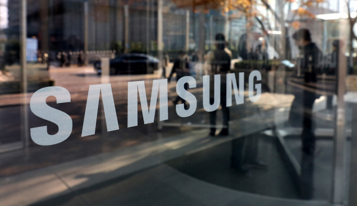
Samsung Electronics Co. has established a new semiconductor research center in Japan, combining two existing research and development institutes into one, to advance its chip technologies and hire more talented R&D staff.
The South Korean tech giant restructured its two R&D facilities – one in Yokohama and the other in Osaka – late last year to launch an enlarged semiconductor research and development center in Japan, dubbed DSRJ.
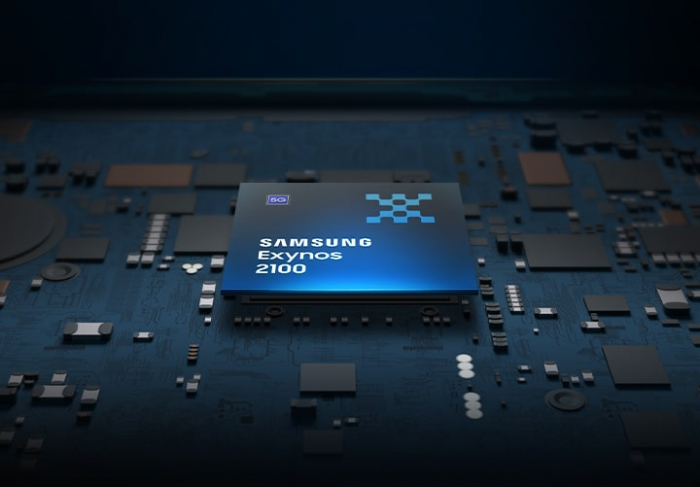
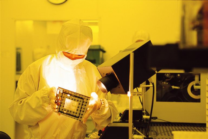
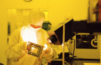
The new research center will play the role of Samsung’s R&D control tower in Japan with a focus on the design and development of system LSI chips such as image sensors, application processors (APs) and modems.
Samsung, the world’s largest memory chipmaker and the No. 2 foundry player after Taiwan’s TSMC, has been strengthening its research capabilities as demand for semiconductors grows across various industries, including artificial intelligence, autonomous vehicles and 5G communications.
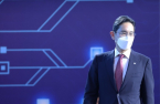
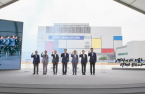
Samsung Electronics Chairman Lee Jae-yong, known as Jay Y. Lee in the West, said last week during his trip to the company’s chip research institute in Hwaseong, Gyeonggi Province that the chipmaker aims to double its research capabilities in both quality and quantity terms over the next few years.
Last year, Samsung unveiled a plan to spend 20 trillion won ($15.3 billion) by 2028 to build a new semiconductor R&D complex in Giheung, Gyeonggi Province for the development of next-generation memory and system chip technologies.
TOKYO DECLARATION
Industry watchers said Samsung’s history of its chip business dates back to the early 1980s when its founder Lee Byung-chull publicly announced the company's entry into the semiconductor industry through what is called the Tokyo Declaration.
He is said to have made up his mind to start a chip manufacturing business with advice from Dr. Inaba Hidezo of Keidanren, Japan’s business federation.
In recent years, however, Samsung’s Japan business has been put on the back burner amid the strained relationship between Korea and Japan.
The Korean chipmaker now hopes to revitalize its Japan business by bolstering its R&D capabilities and aggressively recruiting talented researchers in the neighboring country.
In a related move, Kyung Kye-hyun, Samsung's semiconductor business chief, earlier this week met with Sony Chairman Kenichiro Yoshida to discuss potential cooperation at Samsung’s Pyeongtack plant.
Samsung’s move to strengthen its chip business in Japan comes as Korean President Yoon Suk Yeol is set to embark on a two-day trip to Tokyo Thursday for a summit meeting with Prime Minister Kishida Fumio on ways to improve bilateral relations.
Next month, Yoon is also traveling to the US to meet with President Joe Biden over tricky issues involving the CHIPS and Science Act and the Inflation Reduction Act.
Write to Ji-Eun Jeong at jeong@hankyung.com
In-Soo Nam edited this article.
More to Read
-
 Korean chipmakersSamsung’s Jay Y. Lee walks on tightrope in US, China investments
Mar 14, 2023 (Gmt+09:00)
4 Min read -
 Korean chipmakersSamsung chief Lee vows bold investment to bolster chip R&D capabilities
Mar 14, 2023 (Gmt+09:00)
2 Min read -
 Korean chipmakersKorea to raise young chip engineers for Samsung, SK Hynix
Mar 13, 2023 (Gmt+09:00)
3 Min read -
 Business & PoliticsYoon’s US visit to test Biden’s trust as ally over chip, battery issues
Mar 08, 2023 (Gmt+09:00)
3 Min read
Comment 0
LOG IN