Korean chipmakers
Samsung chief Lee vows bold investment to bolster chip R&D capabilities
The world’s largest memory chip producer expedites R&D funding to maintain technology leadership
By Mar 14, 2023 (Gmt+09:00)
2
Min read
Most Read
LG Chem to sell water filter business to Glenwood PE for $692 million


Kyobo Life poised to buy Japan’s SBI Group-owned savings bank
KT&G eyes overseas M&A after rejecting activist fund's offer
StockX in merger talks with Naver’s online reseller Kream
Mirae Asset to be named Korea Post’s core real estate fund operator


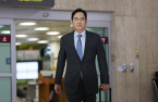
Samsung Electronics Co. Chairman Jay Y. Lee pledged another bold investment in the world’s largest memory chipmaker’s next-generation semiconductor research and development to further widen the gap with its rivals in the latest chip industry downturn.
“The company will strive to ‘double’ our semiconductor R&D capability quantitatively and qualitatively,” Lee told R&D engineers and researchers on Friday during his visit to Samsung Electronics’ Semiconductor Research & Development (SRD) center in the company’s Hwaseong campus in Korea.
Lee’s latest visit to the SRD center underscores his commitment to maintaining a major gap between Samsung Electronics and its peers with unparalleled technologies.
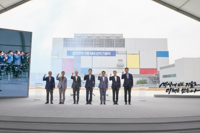
The Korean chip giant unveiled another investment plan to spend 20 trillion won ($15.3 billion) by 2028 to build its new semiconductor R&D complex in Giheung for the development of next-generation memory and system chip technologies during its ground-breaking ceremony in August last year.
“Let’s build the future through unprecedented technologies with a technology-centric mindset and advanced investments,” Lee was quoted as saying during the ceremony.
MRAM DEVELOPMENT IS SRD’S PRIORITY
The SRD is at the center of Samsung Electronics’ next-generation chip development by leading the research and development of chip technologies that the company can commercialize in one to two years. Another of its research centers, Samsung Advanced Institute of Technology (SAIT), is responsible for developing new technologies that can lead the industry in the next five to 10 years.
Lee showed particular interest in magnetic random-access memory (MRAM) chips during his visit to the Hwaseong research complex last week, hoping that Samsung Electronics can further prove its global leadership by becoming the first company to commercialize MRAM chips.
The MRAM chip stores data bits using magnetic states instead of electrical charges, and it is touted as a game changer that can offset the limitations of dynamic random-access memory and NAND flash memory chip technologies.
MRAM chips' data processing rate is 10 times faster than that of DRAM and NAND flash chips but their production cost is lower, and their lifetime is longer.
Since Lee was inaugurated as Samsung Electronics’ chairman in October last year, he has visited many of Samsung’s R&D centers across the world to encourage researchers and engineers and inspect the company’s technology prowess, reaffirming his commitment to technology leadership amid intensifying competition.
The company has also been aggressively recruiting R&D staff with doctoral degrees from around the world to bolster its R&D capabilities.
Last year it unveiled an ambitious plan to lead the global foundry market with the development of 1.4-nanometer chips by 2027 while pledging 7.5 trillion won worth of investments in the bio sector until 2023 to repeat the success of its semiconductor business.
Write to Jeong-Soo Hwang at hjs@hankyung.com
Sookyung Seo edited this article.
More to Read
-
 Tech, Media & TelecomSamsung Chairman Jay Y. Lee flies to Vietnam for global business
Dec 21, 2022 (Gmt+09:00)
1 Min read -
 Leadership & ManagementJay Y. Lee inaugurated as chairman of Samsung Electronics
Oct 27, 2022 (Gmt+09:00)
1 Min read
Comment 0
LOG IN