Foundry competition
Samsung to make 2-nanometer GAA chips by 2025 to overtake TSMC
The technology advancement comes as Samsung is striving to narrow the market-share gap with the foundry leader
By Oct 07, 2021 (Gmt+09:00)
3
Min read
Most Read
S.Korea's LS Materials set to boost earnings ahead of IPO process


Samsung shifts to emergency mode with 6-day work week for executives
NPS to commit $1.1 billion to external managers in 2024
HD Hyundai Marine IPO sees strong demand from retail investors
Navigating choppy waters: Dollar-won FX forecasting ┬Ā


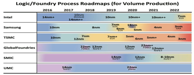
Samsung Electronics Co. said on Thursday it will be able to commercialize a 2-nanometer transistor process technology by 2025 to take on bigger foundry rival Taiwan Semiconductor Manufacturing Co. (TSMC) at the leading edge of chip processing.
At the Samsung Foundry Forum 2021, the South Korean tech giant said it aims to mass produce 2 nm chips based on its proprietary gate-all-around (GAA) transistor architecture from 2025.
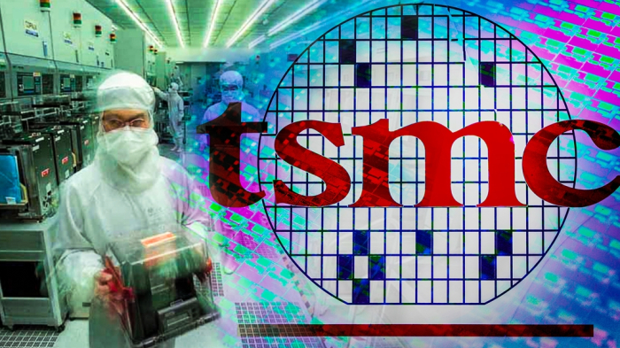
TSMC, the foundry market leader, has yet to unveil its roadmap for 2 nm chip volume production, industry officials said.
During the online event on Thursday, Samsung also said it will begin mass production of its first-generation 3 nm chips in the first half of next year, around the same time TSMC plans to manufacture those chips in large quantities. Samsung said its second-generation 3 nm-based chip design will be available in 2023.
Samsung earlier said it will likely adopt the 3 nm technology by the end of 2022.
If Samsung introduces the advanced process technology ahead of its bigger rival, it will appeal to major global clients such as Google, Qualcomm and Apple, officials said.
TSMC is known to be launching 3 nm chip process equipment at its main plant in Taiwan this year with an aim to start volume production in July 2022.
The GAA architecture, a next-generation foundry microfabrication process, is a key technology that improves electrostatic properties that translate into increased performance, reduced power and optimal chip designs, according to Samsung.
Back in 2019, the company detailed how the 3 nm node would enable it to fabricate items with advantages. It said the 3 nm GAA would offer a 30% performance boost, a 50% decrease in energy consumption and a 35% reduction in chip area, compared to the 5 nm process.
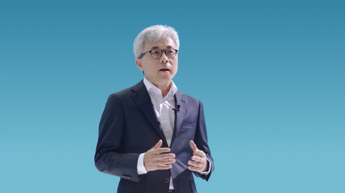
ŌĆ£Through a large-scale investment, we are going to achieve drastic innovations in micro-process technology,ŌĆØ said Choi Si-young, head of SamsungŌĆÖs foundry business, during the forum, an annual gathering of the chipmakerŌĆÖs clients and partners.
CUT-THROAT COMPETITION
SamsungŌĆÖs announcement that it will accelerate its technology advancement roadmap comes as the company is struggling to narrow the market-share gap with TSMC.
According to market research firm Counterpoint Research, Samsung, as the worldŌĆÖs second-largest foundry player, controlled 14% of the global foundry market in terms of revenue, far behind TSMCŌĆÖs 58% share, in the second quarter.
The gap widened from the first quarter, when Samsung commanded 17% of the market, while the Taiwanese company had a 55% share.
TSMC has said it will invest $100 billion in its foundry business over the next three years to consolidate its market leadership.
SamsungŌĆÖs widening gap with TSMC also comes as US tech giant Intel Corp. is throwing down the gauntlet to jump into the foundry business, a growing sector that manufactures cutting-edge chips for fabless firms, including chip designers.
While announcing billions of dollars of investment in the chip business in March, Intel said it aims to produce a 1.8 nm chip by 2024 ŌĆō a move industry watchers say could be far-fetched.
Electric vehicle makers and tech companies such as Tesla and Apple have also said they will produce auto chips in-house to reduce their dependence on chipmakers.
The global foundry market is forecast to grow to $151.2 billion by 2025 from $107.2 billion this year, according to semiconductor market research firm IC Insights.
SAMSUNGŌĆÖS 17-NANOMETER FINFET
Under SamsungŌĆÖs Vision 2030 announced in April 2019, the company plans to invest a total of 133 trillion won to become the worldŌĆÖs top foundry player by then.
The company is known to be spending over 10 trillion won ($8.5 billion) annually in its foundry business alone since 2019 to close in on TSMC.
At its foundry forum on Thursday, Samsung also unveiled its plan to use a 17-nanometer fin field-effect transistor (FinFET) process to make chips for image sensors and mobile display driver ICs.
Compared to the existing 28 nm node, the 17 nm technology will ensure a 39% performance boost, a 49% cut in power consumption and a 43% reduction in chip area, according to Samsung.
Write to Shin-Young Park and Su-Bin Lee at nyusos@hankyung.com
In-Soo Nam edited this article.
More to Read
-
![[Exclusive] Samsung to make TeslaŌĆÖs HW 4.0 self-driving auto chip](/data/ked/image/2021/09/23/ked202109230030.145x94.0.jpg) [Exclusive] Semiconductors[Exclusive] Samsung to make TeslaŌĆÖs HW 4.0 self-driving auto chip
[Exclusive] Semiconductors[Exclusive] Samsung to make TeslaŌĆÖs HW 4.0 self-driving auto chipSep 23, 2021 (Gmt+09:00)
4 Min read -
 TechSamsung unveils industryŌĆÖs first 5 nm processor for wearable devices
Aug 10, 2021 (Gmt+09:00)
2 Min read -
 Foundry competitionSamsung, TSMC in heated race for industryŌĆÖs smallest 3 nm process node
Aug 04, 2021 (Gmt+09:00)
4 Min read -
 Foundry competitionSamsung, TSMC up ante in US foundry competition
May 24, 2021 (Gmt+09:00)
3 Min read -
 Foundry competitionIntelŌĆÖs jump into foundry sets off alarm bells for Samsung, TSMC
Mar 24, 2021 (Gmt+09:00)
3 Min read
Comment 0
LOG IN