Korean chipmakers
Korea to inject $200 mn into semiconductor packaging R&D
South Korea lags far behind Taiwan, China and US in the semiconductor packaging market
By Jun 26, 2024 (Gmt+09:00)
2
Min read
Most Read
LG Chem to sell water filter business to Glenwood PE for $692 million


KT&G eyes overseas M&A after rejecting activist fund's offer
Kyobo Life poised to buy Japan’s SBI Group-owned savings bank
StockX in merger talks with Naver’s online reseller Kream
Meritz backs half of ex-manager’s $210 mn hedge fund


South Korea will inject 274.4 billion won ($200 million) into a state-run R&D project for semiconductor packaging technology, a key to producing the high-performance, low-power chips essential for AI applications.
The government spending aims to narrow the gap with Taiwan, China and the US in the semiconductor back-end process market, where Korea controls less than 10%. In contrast, it commands 60% of the memory chip market as of 2022, according to the Ministry of Science and ICT.
The Ministry of Trade, Industry and Energy said on Wednesday the R&D spending plan had passed the preliminary feasibility test conducted by the science ministry. That means the government has given the go-ahead to the seven-year project running until 2031.
The plan represents a follow-up to a 65-billion-won, state-run project on semiconductor packaging R&D undertaken between 2018 and 2022.
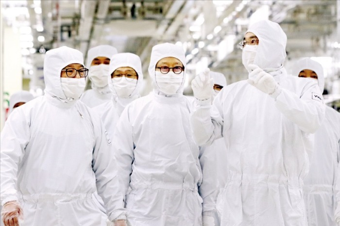
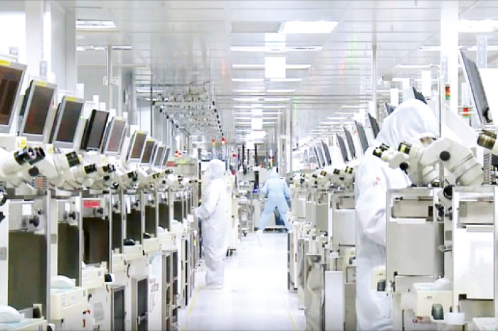
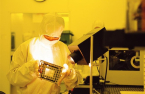
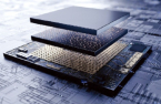
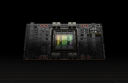
Packaging refers to assembling different types of semiconductor chips and providing them to customers in one piece.
The process involves detaching chips through wafer sawing and mounting the chips on a module that will be installed onto a motherboard. The package allows the chips to be electrically and mechanically connected to external components.
To meet the growing demand for high-end chips such as high bandwidth memory (HBM) amid the AI boom, chipmakers are focusing on improving back-end processing or packaging technology now that semiconductor miniaturization has reached its physical limits.
The advanced semiconductor packaging market is forecast to expand at a compounded annual growth rate of 10% to $78.6 billion by 2028, from $44.3 billion in 2022, according to research company Yole.
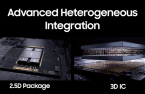
Samsung Electronics will launch three-dimensional (3D) packaging services for HBM chips within the year, according to the company and industry sources earlier this month.
To do so, its advanced packaging team will vertically interconnect HBM chips produced at its memory business division with GPUs assembled for fabless companies by its foundry unit.
3D packaging reduces power consumption and processing delays, improving the electrical signal quality of semiconductor chips.
Presently, HBM chips are horizontally connected with a GPU on a silicon interposer via the 2.5D packaging process.
Write to Yeong-Hyo Jeong at hugh@hankyung.com
Yeonhee Kim edited this article
More to Read
-
 Korean chipmakersBooming AI industry boosts chip packaging equipment makers
Jun 24, 2024 (Gmt+09:00)
3 Min read -
 Korean chipmakersSamsung to launch 3D HBM chip packaging service in 2024
Jun 16, 2024 (Gmt+09:00)
2 Min read -
 Korean chipmakersSK Hynix to build advanced packaging plant in Indiana for $3.9 bn
Apr 04, 2024 (Gmt+09:00)
4 Min read -
 Korean chipmakersHana Micron to develop 2.5D packaging for Nvidia’s H100 AI chip: CEO
Feb 29, 2024 (Gmt+09:00)
3 Min read -
 Korean chipmakersSamsung to build $281 million chip packaging R&D center in Yokohama
Dec 22, 2023 (Gmt+09:00)
3 Min read -
 Korean chipmakersSamsung to relocate packaging unit workplace to lure talent
Dec 14, 2023 (Gmt+09:00)
3 Min read -
 Korean chipmakersSamsung to unveil 3D AI chip packaging tech SAINT to rival TSMC
Nov 12, 2023 (Gmt+09:00)
3 Min read -
 Korean chipmakersSamsung set to supply HBM3, packaging services to AMD
Aug 22, 2023 (Gmt+09:00)
1 Min read -
 Korean chipmakersSamsung Elec to provide HBM3, packaging service to Nvidia
Aug 01, 2023 (Gmt+09:00)
5 Min read
Comment 0
LOG IN