Korean chipmakers
SK Hynix to build advanced packaging plant in Indiana for $3.9 bn
This would be the S.Korean chipmaker’s first chip plant in the US, also the industry’s first advanced packaging plant there
By Apr 04, 2024 (Gmt+09:00)
4
Min read
Most Read
LG Chem to sell water filter business to Glenwood PE for $692 million


KT&G eyes overseas M&A after rejecting activist fund's offer
Kyobo Life poised to buy Japan’s SBI Group-owned savings bank
StockX in merger talks with Naver’s online reseller Kream
Meritz backs half of ex-manager’s $210 mn hedge fund


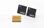
SK Hynix Inc., the world’s leading high bandwidth memory (HBM) chip producer, will plow in $3.87 billion to build advanced packaging and research and development facilities for AI chips in Indiana, which would be the first of its kind in the US and the company’s first overseas HBM chip plant.
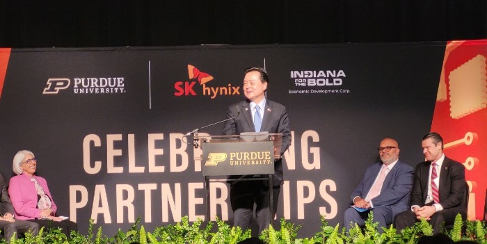
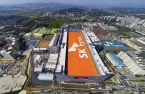
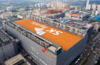
According to a press release by SK Hynix on Thursday, the South Korean chip giant signed an investment agreement the day before with the State of Indiana, Purdue University and the US government to build advanced chip packaging and R&D facilities in West Lafayette, Indiana with an investment of $3.87 billion.
At the plant, the company will produce HBM chips and leverage talent from Purdue University, also in West Layfayette, famous for its strong semiconductor and hardware AI R&D capabilities and experts, to develop next-generation chip technology.
The company aims to start mass-producing the high-performance, high-value memory chips, essential components in running graphics processing units (GPU) that train AI systems like ChatGPT, in the second half of 2028.
This marks the first attempt to build an advanced packaging facility for AI chips in the US. It is also the company’s first-ever US chip plant and first HBM-producing facility abroad.
“We are excited to become the first in the industry to build a state-of-the-art advanced packaging facility for AI products in the United States that will help strengthen supply-chain resilience and develop a local semiconductor ecosystem,” SK Hynix Chief Executive Officer Kwak Noh-Jung said at an agreement signing ceremony.
“With this new facility, we hope to advance our goal of providing AI memory chips with unmatched capabilities, serving the needs of our customers.”
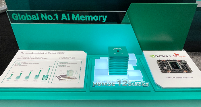
SK Hynix commands the global HBM chip market with about 50% share, ahead of its bigger memory rival Samsung Electronics Co., according to TrendForce. In the latest-generation HBM3 market, SK Hynix holds over 90% share.
It currently supplies its HBM chips to the world’s most famous AI chip company Nvidia Corp.
TO CEMENT LEADERSHIP IN THE HBM MARKET
The new advanced packaging plant in the US is expected to enable SK Hynix to get more high-performance chip orders from its key US customers, including Nvidia, Apple Inc. and Advanced Micro Devices Inc. (AMD), as it will be closer to them.
Under the US CHIPS and Science Act enacted in 2022, the new US plant will allow it to tap into generous government tax breaks aimed at bolstering the country’s semiconductor industry.
Under the Act, any semiconductor company that builds a production facility in the US can benefit from the US government’s subsidies worth $39 billion and $13.2 billion for R&D for five years.
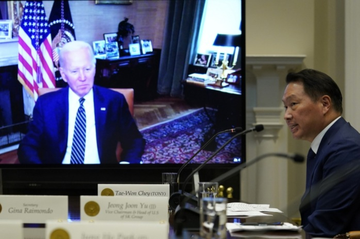
Hoping to enjoy the benefits, Chey Tae-won, the chairman of SK Group, SK Hynix’s parent, vowed in July 2022 to build the group’s first memory chip packaging facility in the US as part of a $22 billion investment in the US manufacturing sector.
Its crosstown rival Samsung Electronics is expected to be granted more than $6 billion in US subsidies for its new chip foundry plant in Taylor, Texas.
SK Hynix is said to have already submitted a tax break application for the new packaging plant in Indiana to the US government.
“SK Hynix will soon be a household name in Indiana,” US Senator Todd Young said at the signing ceremony. “The CHIPS and Science Act opened a door that Indiana has been able to sprint through, and companies like SK Hynix are helping to build our high-tech future.”
The Korean chipmaker expects its first-ever US chip plant to drive innovation in the AI supply chain in the US and create more than a thousand new jobs in the region.
“It is also a monumental moment for completing the supply chain of the digital economy in our country through chips advanced packaging. Located at Purdue Research Park, the largest facility of its kind at a US university will grow and succeed through innovation,” said Purdue University President Mung Chiang.
AGGRESSIVE INVESTMENTS
As a HBM leader, SK Hynix will expedite its investments in chip production facilities across the world.
It recently announced a plan to spend 120 trillion won ($89 billion) to construct the world’s largest chip production facilities, dubbed the Yongin Semiconductor Cluster, in Korea.
The company plans to break ground on the first fab in March of 2025 to complete the construction of the entire campus by early 2027.
It also plans to build a mini fab, a facility with equipment for 300-millimeter wafer processing, to test semiconductor materials, components and equipment.
Its announcement to build the advanced packaging plant comes about a month after the Financial Times reported that Indiana was picked as the home to SK Hynix’s US advanced packaging plant. Indiana had been floated as one of three strong candidates along with Arizona and Texas.
At the time, SK Hynix declined to confirm the report.
SK Hynix currently has an R&D center in San Jose, California and sales offices across the US without operating a manufacturing facility in the country.
SK Hynix shares rose 4.4% to trade at 187,100 won in a mid-afternoon session on Thursday.
Write to Jeong-Soo Hwang at hjs@hankyung.com
Sookyung Seo edited this article.
More to Read
-
 Korean chipmakersSK Hynix earmarks $91 bn to construct world's largest chip fab
Mar 21, 2024 (Gmt+09:00)
1 Min read -
 Korean chipmakersSK Hynix mass-produces HBM3E chip to supply Nvidia
Mar 19, 2024 (Gmt+09:00)
3 Min read -
 Korean chipmakersSK Hynix to build US chip packaging plant in Indiana: FT
Feb 01, 2024 (Gmt+09:00)
2 Min read -
 EarningsSK Hynix swings to profit; sees 60% surge in HBM demand
Jan 25, 2024 (Gmt+09:00)
3 Min read -
 Korean chipmakersSamsung, SK Hynix join forces with foreign rivals to win AI chip war
Dec 31, 2023 (Gmt+09:00)
4 Min read
Comment 0
LOG IN