Korean chipmakers
Samsung, ASML to build joint research plant in Hwaseong
They will install ASML’s high NA EUV system in the new lab to develop next-generation EUV technologies for smaller nodes
By Dec 15, 2023 (Gmt+09:00)
3
Min read
Most Read
LG Chem to sell water filter business to Glenwood PE for $692 million


KT&G eyes overseas M&A after rejecting activist fund's offer
Kyobo Life poised to buy Japan’s SBI Group-owned savings bank
StockX in merger talks with Naver’s online reseller Kream
Meritz backs half of ex-manager’s $210 mn hedge fund


“Our main goal is to build a joint research lab in Dongtan, where Samsung and ASML engineers will collaborate to develop (next-generation EUV) technologies with (ASML’s) high-numerical aperture extreme ultraviolet lithography (high NA EUV) system,” Samsung Electronics Device Solutions Division Chief Executive Kyung Kye-hyun told reporters at Seoul's Gimpo Airiport on Friday upon returning from the Netherlands as part of Korean President Yoon Suk Yeol’s business delegation.
The two companies signed a memorandum of understanding earlier this week during President Yoon’s four-day state visit to the European country to invest 1 trillion won ($760 million) to build a research plant in Korea to jointly develop next-generation extreme ultraviolet lithography (EUV) technology.
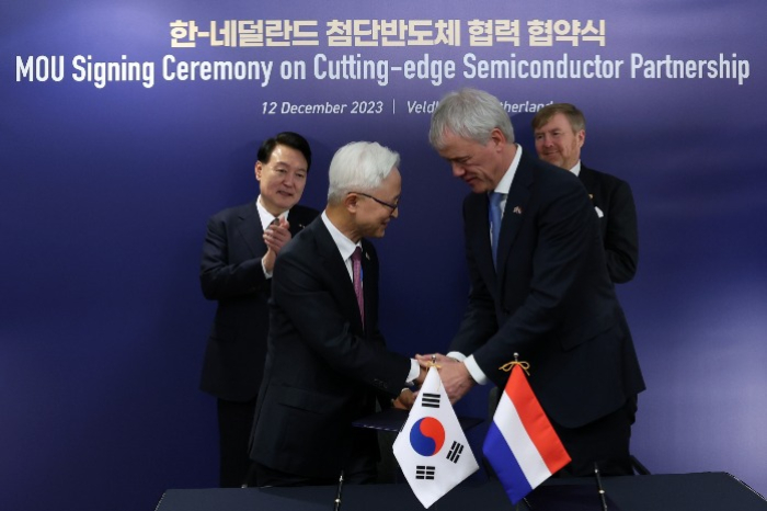
It is the first time for the joint lab's location to be revealed.
Dongtan is in Hwaseong, where Samsung Electronics has one of its major local semiconductor manufacturing campuses and a R&D center. ASML Korea’s office is also located near the Samsung campus in the town.
HIGH NA EUV, KEY FOR 2NM PROCESS
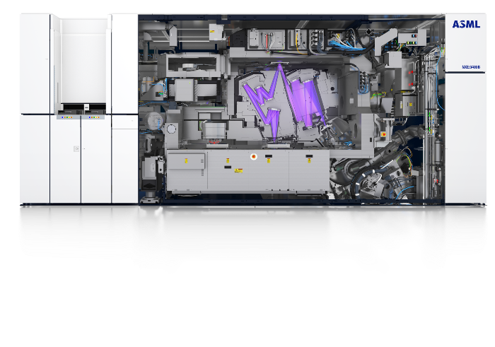
The high NA EUV developed by ASML is a promising EUV technology that is expected to enable the development and production of chips at nodes even smaller than 2 nanometers, which Samsung Electronics and its bigger foundry rival Taiwan Semiconductor Manufacturing Company Ltd. (TSMC) are fiercely competing to secure.
The machine uses lasers beyond the ultraviolet end of the spectrum to etch pathways for circuity on a minute scale.
ASML is the world’s sole producer of EUV lithography machines, which allow chip producers to shrink the size of transistors down to just a few nanometers, tens of thousands of times thinner than a strand of human hair.
Samsung Electronics is aggressively seeking to commercialize 2nm chips by 2025 after mass-producing 3nm chips last year.
The Korean chip giant expects its enhanced partnership with ASML will enable it to secure next-generation EUV technology, crucial to developing high-end chips required to run artificial intelligence-powered devices.
“Our latest agreement is expected to allow Samsung Electronics priority access to high NA EUV technology, and will pave the way for the use of high NA EUV in DRAM in the long term,” said Kyung.
“As EUV lithography is the most important tool (in semiconductor production), we have earned a very powerful key ally in the global chip supply chain," added Kyung, speaking of the agreements signed during President Yoon’s state visit to the Netherlands.
ASML also pins high hopes on its joint research facility in Korea, the home to the world’s top two memory chip makers Samsung Electronics and SK Hynix Inc., for the development of next-generation EUV technologies.
When completed, the joint R&D facility will mark the Veldhoven, Netherlands-based company’s first overseas research facility jointly established with a semiconductor company.
The new plant will also expand ASML’s presence in Korea, where it already has four sites, including the one in Dongtan, which serve customers including Samsung.
Write to Jeong-Soo Hwang at hjs@hankyung.com
Sookyung Seo edited this article.
More to Read
-
 Korean chipmakersASML, Samsung to build R&D center in Korea for $760 mn
Dec 13, 2023 (Gmt+09:00)
3 Min read -
 Korean chipmakersSamsung Electronics makes 17-fold gains from investment in ASML
Jun 05, 2023 (Gmt+09:00)
3 Min read -
 Korean chipmakersSamsung to make 3 nm chips for Nvidia, Qualcomm, IBM, Baidu
Nov 22, 2022 (Gmt+09:00)
3 Min read -
 Korean chipmakersSamsung to make 2-nanometer GAA chips by 2025 to overtake TSMC
Oct 07, 2021 (Gmt+09:00)
3 Min read
Comment 0
LOG IN