Korean chipmakers
Samsung eyes next-generation 5 nm eMRAM auto chip by 2027
The top memory chipmaker also aims to advance its power chip tech for EVs and autonomous vehicles
By Oct 19, 2023 (Gmt+09:00)
3
Min read
Most Read
LG Chem to sell water filter business to Glenwood PE for $692 million


Kyobo Life poised to buy Japan’s SBI Group-owned savings bank
KT&G eyes overseas M&A after rejecting activist fund's offer
StockX in merger talks with Naver’s online reseller Kream
Mirae Asset to be named Korea Post’s core real estate fund operator


Samsung Electronics Co., the world’s largest memory chipmaker, said on Thursday it aims to develop a next-generation 5-nanometer-processed automotive memory chip, called eMRAM, by 2027.
While unveiling its technology roadmap for the advanced memory chip, the South Korean tech giant also said it will drastically improve processing nodes for power chips to prepare for the era of electric cars and autonomous vehicles.
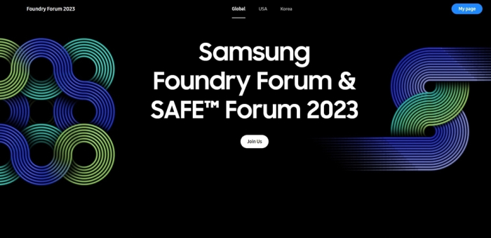
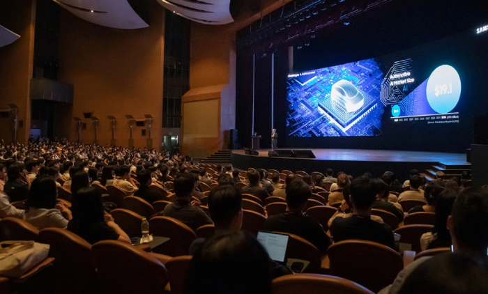
Hosting the Samsung Foundry Forum (SSF) and Samsung Advanced Foundry Ecosystem (SAFE) Forum 2023 in Munich, Germany, the company said it is setting its sights on auto chips as a key growth driver.
In 2019, Samsung Foundry, the Korean chipmaker’s contract chipmaking unit, became the industry’s first to mass-produce an eMRAM chip on a 28 nm process node.
Short for embedded magnetic random access memory, eMRAM is the next-generation core memory semiconductor for automotive applications that operates stably even at high temperatures thanks to its fast read and write speeds.
The company is currently developing a 14 nm eMRAM based on the fin field-effect transistor (FinFET) structure with an aim to unveil it by 2024.
Samsung plans to expand its eMRAM portfolio to 8 nm products by 2026 and 5 nm products by 2027.
The company said 8 nm eMRAM chips will offer a 30% higher density and are 33% faster compared to such chips produced using the 14 nm technology.
Separately, Samsung said it will make preparations to begin mass production of cutting-edge 2 nm-processed auto chips by 2026.
According to market research firm Omdia, the global automotive chip market is forecast to grow to $96.2 billion by 2026 from $63.5 billion in 2022.
“We will develop processes optimized for automotive semiconductors, including power chips and microcontroller units, to meet various customer needs in the era of EVs and autonomous vehicles,” said Samsung’s foundry business chief Choi Si-young.
TO STRENGTHEN 8-INCH BCD PROCESS
Samsung said it will also sharpen its technology for the 8-inch BCD process.
BCD, short for bipolar, CMOS and DMOS, is a set of silicon processes, each of which combines the strengths of three different process technologies onto a single chip.
This combination of technologies brings many advantages – improved reliability, reduced electromagnetic interference and smaller chip area. BCD has been widely adopted and continuously improved to address a broad range of products and applications in the fields of power management, analog data acquisition and power actuators.
Samsung, which currently employs the 130 nm BCD process, aims to advance the technology to the 90-nanometer level by 2025. The 90 nm BCD process can reduce chip area by about 20% compared with the 130 nm process.
Utilizing the deep trench isolation (DTI) technology, Samsung plans to increase the voltage applied to automotive solutions from the current 70 volts to 120 volts, and it intends to provide a process design kit for the 130 nm BCD process with 120 volts by 2025.
2.5D & 3D PACKAGE DEVELOPMENT WITH PARTNERS
At the Munich forum, Samsung said it will closely cooperate with its partners for chip packaging, aiming to develop 2.5D and 3D packaging tailored to various applications, including high-performance computing.
Within its SAFE ecosystem, Samsung, along with 20 chip business partners, has established the Multi Die Integration (MDI) Alliance for cutting-edge packaging solutions.
At its foundry forum held in Seoul in July, Samsung said it is bolstering partnerships with its clients to enhance its presence in the foundry segment, in which it is a distant second behind market leader Taiwan Semiconductor Manufacturing Co. (TSMC), which controls more than half of the global market.
Samsung has been striving to expand its foundry client base with its advanced chip processing technology, particularly in the fast-growing auto chip segment.
In February, Samsung clinched a deal to make auto chips for US chip designer Ambarella Inc., using its advanced 5 nm process node.
Write to Jeong-Soo Hwang at hjs@hankyung.com
In-Soo Nam edited this article.
More to Read
-
 Korean chipmakersSamsung narrows gap with TSMC in foundry market share
Sep 06, 2023 (Gmt+09:00)
3 Min read -
 Korean chipmakersSamsung improves 4 nm foundry yields, on par with TSMC: analyst
Jul 11, 2023 (Gmt+09:00)
4 Min read -
 Korean chipmakersSamsung Electronics to aid foundry clients with state-of-the-art tech
Jul 05, 2023 (Gmt+09:00)
3 Min read -
 Korean chipmakersSamsung on smooth track to 1.4 nm foundry tech to take on TSMC
Jun 28, 2023 (Gmt+09:00)
4 Min read -
 Korean chipmakersSamsung eyes wider foundry client base with Ambarella deal
Feb 21, 2023 (Gmt+09:00)
2 Min read
Comment 0
LOG IN