Korean chipmakers
Samsung’s new NAND boasts industry’s highest storage capacity
The Korean tech giant aims to develop over 1,000-layer NAND chip by 2030 for higher density and storage capabilities
By Nov 08, 2022 (Gmt+09:00)
2
Min read
Most Read
LG Chem to sell water filter business to Glenwood PE for $692 million


KT&G eyes overseas M&A after rejecting activist fund's offer
Kyobo Life poised to buy Japan’s SBI Group-owned savings bank
StockX in merger talks with Naver’s online reseller Kream
Meritz backs half of ex-manager’s $210 mn hedge fund


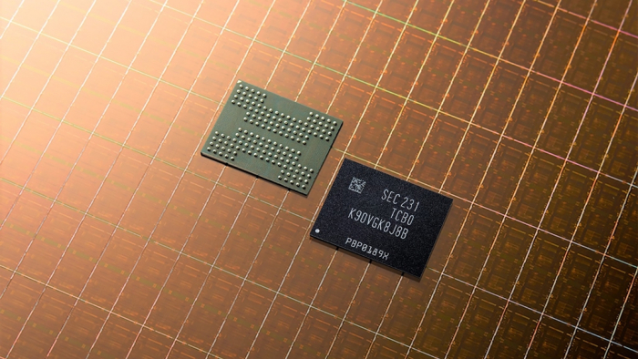
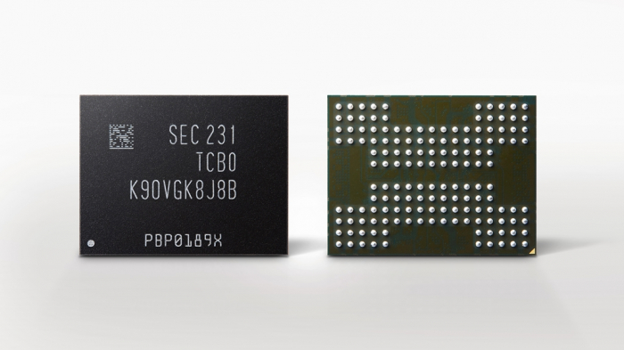
Samsung Electronics Co., the world’s largest memory chipmaker, has begun mass producing its latest NAND chip, which features the industry’s highest storage capacity and highest bit density, suitable for large-scale enterprise servers.
The 1-terabit (Tb) triple-level cell (TLC) eighth-generation vertical NAND (V-NAND) will enable larger storage space in next-generation enterprise server systems, the South Korean tech giant said in a statement on Monday.
Industry watchers said the new NAND chip will likely be 236-layered to achieve the industry’s highest density, although Samsung didn’t confirm it.
In July 2021, Samsung said it made significant progress in developing a 200-layer V-NAND flash memory.
Company executives said at the time that it secured the technology to produce 200-layer and higher stacked eighth-generation V-NAND chips and is preparing for a production line ramp-up.
Samsung said on Monday it was able to attain the industry’s highest bit density by significantly enhancing the bit productivity per wafer.
LATEST FLASH STANDARD
Based on the Toggle DDR 5.0 interface – the latest NAND flash standard – Samsung’s eighth-generation V-NAND features an input and output speed of up to 2.4 gigabits per second (Gbps), 1.2 times faster than its previous seventh-generation NAND chip unveiled last year.
“As market demand for denser, greater-capacity storage pushes for higher V-NAND layer counts, Samsung has adopted its advanced 3D scaling technology to reduce surface area and height, while avoiding the cell-to-cell interference that normally occurs with scaling down,” said Hur Sung-hoi, executive vice president of Samsung’s flash product and technology division.
NAND chips are flash memory chips, which store data even when power is turned off and are used in devices like smartphones, USB drives and servers.
Samsung has been the NAND market leader since 2002.
The company aims to move to the ninth-generation V-NAND in 2024 and develop over 1,000-layer NAND chips by 2030.
Samsung’s rivals are also unveiling high-density NAND chips.
Micron Technology Inc. said in July it has begun producing 232-layer NAND chips in large quantities.
SK Hynix Inc., the world's second-largest memory chipmaker, said in August it has shipped samples of the industry’s highest density 238-layer, 512-gigabit (Gb) four-dimensional NAND chip to customers, with a plan to start mass production in the first half of 2023.
Write to Ji-Eun Jeong at jeong@hankyung.com
In-Soo Nam edited this article.
More to Read
-
 Korean chipmakersSamsung’s $22 bn new chip plant up and running to make NAND flash
Sep 07, 2022 (Gmt+09:00)
3 Min read -
 Korean chipmakersSK Hynix unveils world's first 238-layer NAND; Samsung SSD 20 times faster
Aug 03, 2022 (Gmt+09:00)
3 Min read -
 Korean chipmakersSamsung, SK Hynix ahead of rivals in 200-plus-layer NAND chips
Feb 04, 2022 (Gmt+09:00)
3 Min read -
 EarningsSamsung works on industry’s first 200-layer NAND as its Q2 profit jumps
Jul 29, 2021 (Gmt+09:00)
3 Min read
Comment 0
LOG IN