Korean chipmakers
Samsung vows to regain chip lead with new R&D center
Samsung Electronics will invest 20 trillion won by 2030 in its new R&D complex in South Korea
By Nov 18, 2024 (Gmt+09:00)
3
Min read
Most Read
LG Chem to sell water filter business to Glenwood PE for $692 million


KT&G eyes overseas M&A after rejecting activist fund's offer
Mirae Asset to be named Korea Post’s core real estate fund operator
StockX in merger talks with Naver’s online reseller Kream
Meritz backs half of ex-manager’s $210 mn hedge fund


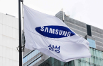
Samsung Electronics Co. is pinning its hopes on its new research and development complex, which will cost the company 20 trillion won ($14.4 billion), in order to regain chip market share after losing ground to its smaller cross-town rival SK Hynix Inc. in a high-bandwidth memory war.
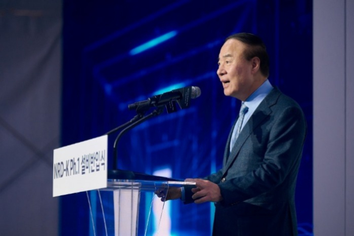
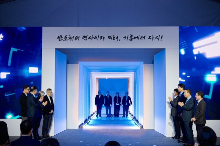
“NRD-K will bolster our development speed, enabling the company to create a virtuous cycle to accelerate fundamental research on next-generation technology and mass production,” Jun Young-hyun, vice chairman and head of the Device Solutions Division at Samsung Electronics, said at a ceremony held Monday to celebrate the start of equipment installation at Samsung’s new R&D complex, dubbed NRD-K.
“We will lay the foundation for a new leap forward in Giheung, where Samsung Electronics’ 50-year history of semiconductors began, and create a new future for the next hundred years,” Jun added.
The company will spend 20 trillion won through 2030 on the complex, which is expected to play a critical role in developing and producing next-generation semiconductors such as artificial intelligence chips.
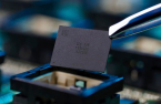
The Korean chip giant – the world’s largest memory chipmaker – lags behind runner-up SK Hynix in an AI chip race. It has not yet passed the world’s No. 1 AI chip maker Nvidia Inc.’s quality test for HBM chips.
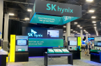
SK Hynix is the world’s leading HBM chip supplier with a market share of 53%, followed by Samsung Electronics with 35%.
With the new R&D center, Samsung Electronics will seek to catch up to SK Hynix in the HBM chip market, which is forecast to grow to $33 billion in 2027 from $4 billion in 2023, according to Morgan Stanley.
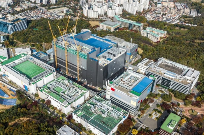
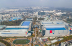
The R&D complex, to be built on a 109,000 square meter footprint at Samsung Electronics' Giheung campus, will house chip development and production R&D facilities under one roof to help speed up next-generation chip development.
It will begin operation of an R&D-dedicated line in mid-2025.
CENTER OF NEXT-GEN CHIP R&D AND PRODUCTION
NRD-K will be equipped with advanced equipment and infrastructure, including high numerical aperture extreme ultra-violet (EUV) lithography and new material deposition equipment, to develop future-leading memory chips such as 3D dynamic random access memory (DRAM) and V-NAND with more than 1,000 layers.
Samsung Electronics will also set up a wafer bonding infrastructure for wafer-to-wafer bonding in the complex.
The cutting-edge R&D complex is also expected to help expand the Korean semiconductor industry’s raw materials, parts and equipment R&D ecosystem considering that Giheung is home to many related companies from around the world, including Korean ones.
“At a time when the importance of win-win partnerships is greater than ever, Applied Materials is committed to accelerating innovation velocity through deep collaboration with Samsung Electronics, working together to drive a new wave of growth for the semiconductor industry,” said Park Gwang-sun, head of Applied Materials Korea.
Samsung Electronics Executive Chairman Jay Y. Lee, during his visit in October last year to the NRD-K construction site, urged employees to mark a turning point for innovation in order to leap forward amid ongoing local and international crises.
Samsung launched its semiconductor business at the Giheung campus in 1983 when the company threw down the gauntlet to larger Japanese chip giants at the time.
Giheung was the birthplace of the world’s first 64-megabyte (Mb) DRAM chips in 1992.
Samsung's chip business head Jun vowed to take drastic steps to improve profitability and regain memory leadership after flagging the company's weaker-than-expected third-quarter earnings in early October.
Write to Eui-Myung Park at uimyung@hankyung.com
Sookyung Seo edited this article.
More to Read
-
 Korean chipmakersSK Hynix, Samsung to cut legacy DRAM output as Chinese firms catch up
Nov 01, 2024 (Gmt+09:00)
4 Min read -
 EarningsSamsung’s memory business fares better in Q3; more HBM sales ahead
Oct 31, 2024 (Gmt+09:00)
5 Min read -
 Korean chipmakersSamsung to unveil 400-layer bonding vertical NAND for AI servers by 2026
Oct 28, 2024 (Gmt+09:00)
3 Min read -
 EarningsSK Hynix’s Q3 profit soars to record high, beats Samsung’s memory profit
Oct 24, 2024 (Gmt+09:00)
4 Min read -
 Korean chipmakersSamsung Apologizes for Falling Behind in AI Chips Race
Oct 10, 2024 (Gmt+09:00)
5 Min read -
 EarningsSamsung chip head vows drastic revamp after flagging weak Q3 earnings
Oct 08, 2024 (Gmt+09:00)
4 Min read
Comment 0
LOG IN