Korean chipmakers
Samsung Lee's urges to keep ‘super gap’ in semiconductor technology
Jay Y. Lee visited the construction site of Samsung’s new chip R&D center before his one-year chairmanship anniversary
By Oct 19, 2023 (Gmt+09:00)
2
Min read
Most Read
LG Chem to sell water filter business to Glenwood PE for $692 million


Kyobo Life poised to buy Japan’s SBI Group-owned savings bank
KT&G eyes overseas M&A after rejecting activist fund's offer
StockX in merger talks with Naver’s online reseller Kream
Mirae Asset to be named Korea Post’s core real estate fund operator


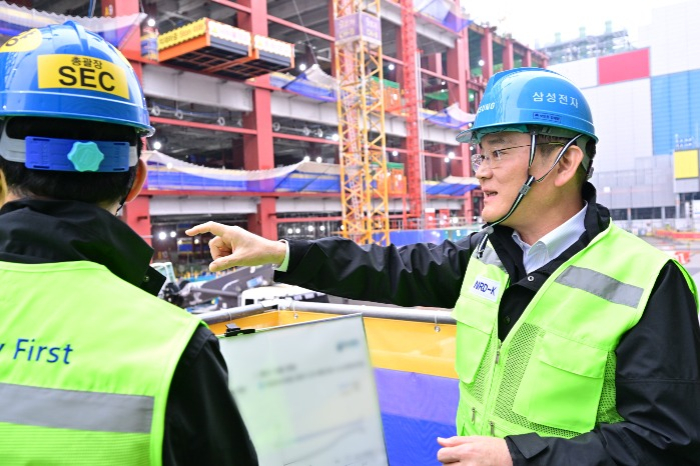
Samsung Electronics Co. Chairman Jay Y. Lee on Thursday visited the construction site of the global memory chip giant’s new semiconductor research & development complex at its Giheung campus, the birthplace of Samsung semiconductors, 14 months after his last visit to the site following his presidential pardon.
His return also happened about a week before the third-year anniversary of his belated father and former Chairman Lee Kun-hee’s death and his own one-year anniversary of chairmanship, underscoring the new chairman’s strong will to keep Samsung’s supremacy over its rivals in semiconductor technology.
“We need a turning point for innovation that leads us to take another leap in the semiconductor business amid ongoing internal and external risks,” Lee said during his inspection of the site, reiterating the importance of maintaining the company's technology leadership and advanced investments.
Lee first visited the construction site during the complex’s groundbreaking ceremony in August last year immediately after he was pardoned by South Korean President Yoon Suk Yeol. He was convicted of bribery and embezzlement in 2017.
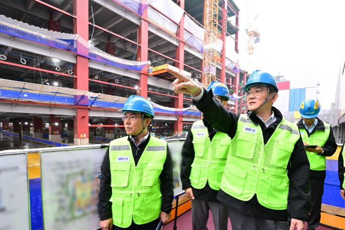
Samsung Electronics plans to invest about 20 trillion won ($14.7 billion) by 2028 for the new R&D complex to lead advanced research on next-generation devices and processes for memory and system chips, as well as to develop innovative technologies for the future.
After the inspection, Lee had a meeting with Samsung Electronics’ Device Solutions Division President and Chief Executive Kyung Kye-hyun, President of the Memory Business Lee Jung-bae and President of the Foundry Business Choi Si-young, who were also joined by other executives.
They mainly discussed current issues in the semiconductor industry such as next-generation processing development, new technology development and the chip supply chain, according to Samsung Electronics.
Samsung Electronics' semiconductor business began at the Giheung campus where the company developed the world’s first 64 Mb dynamic random memory chip (DRAM) in 1992.
Lee will celebrate the one-year anniversary of his chairmanship on Oct. 27.
Write to Jeong-Soo Hwang at hjs@hankyung.com
Sookyung Seo edited this article.
More to Read
-
 Korean chipmakersSamsung eyes next-generation 5 nm eMRAM auto chip by 2027
Oct 19, 2023 (Gmt+09:00)
3 Min read -
 Corporate strategyLate Samsung chairman Lee's New Management back in spotlight
Oct 18, 2023 (Gmt+09:00)
3 Min read -
 Korean chipmakersSamsung chief Lee vows bold investment to bolster chip R&D capabilities
Mar 14, 2023 (Gmt+09:00)
2 Min read -
 Korean chipmakersSamsung to invest $15 bn in semiconductor R&D complex
Aug 19, 2022 (Gmt+09:00)
5 Min read
Comment 0
LOG IN