Korean chipmakers
Samsung to invest $221 mn to build R&D chip line in Japan: Nikkei
The Korean chip giant is expected to use the new chip production facility to develop next-gen chip packaging technologies
By May 15, 2023 (Gmt+09:00)
3
Min read
Most Read
LG Chem to sell water filter business to Glenwood PE for $692 million


KT&G eyes overseas M&A after rejecting activist fund's offer
Mirae Asset to be named Korea Post’s core real estate fund operator
StockX in merger talks with Naver’s online reseller Kream
Meritz backs half of ex-manager’s $210 mn hedge fund


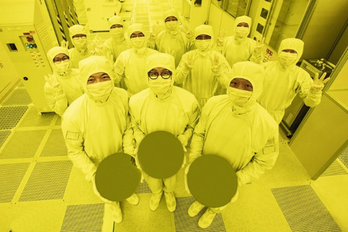
Samsung Electronics Co. will build a prototype chip production facility in Japan for 30 billion yen ($221 million) to develop next-generation back-end chip processing technologies in partnership with Japanese semiconductor materials and equipment producers to further reinforce its foundry capabilities, according to Nikkei Asia on Saturday.
Nikkei Asia reported that the South Korean chip giant, which is also the global memory chip leader, has applied for Japanese government subsidies to build a chip production facility in Yokohama, southwest of Tokyo, with the 30 billion yen investment.
It is expected to receive about 10 billion yen for the construction of the new facility, which is said to produce prototype chips with a focus on the development of next-generation back-end processing technologies, the Japanese media outlet reported, adding that its construction would be completed in 2025.
In response to the Nikkei report, Samsung Electronics said it has been working on the reorganization of its Japanese research and development entity but nothing has yet been determined regarding investment details.
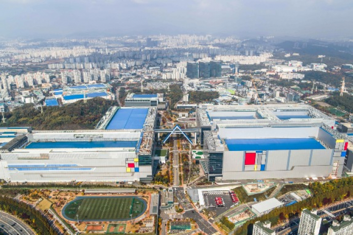
The Korean chip giant in March opened an integrated R&D center for semiconductor and display technologies in Japan, dubbed DSRJ, after combining one center in Yokohama with one in Osaka.
The new Japanese R&D center was set up in Yokohama to play the role of Samsung Electronics’ R&D control tower in Japan with a focus on the development of system LSI chips such as image sensors, application processors and modems.

CHIP PACKAGING TECHNOLOGY
The new chip production facility in the largest port city and technology hub in the Greater Tokyo Area is, however, expected to focus on the R&D of chip back-end processing technologies like packaging, according to the Japanese news site.
Global chip makers have fiercely competed to make chips smaller but faster over the last few decades, but the semiconductor industry now fears that their miniaturization race might have reached its limits, returning chip makers' focus to back-end processing to compete with rivals' products.
Chip production is largely divided into two processes, the front-end and the back-end, and the miniaturization of silicon chips is a part of front-end processing. But following the significant development in chip miniaturization technologies over several decades, making chips tinier is becoming more challenging.
Thus, the latest trend in the chip industry is to improve back-end processing for better chip performance, industry experts said. And stacking wafers into multiple layers is being widely explored in the latest packaging technology development.
TO ENHANCE FOUNDRY CAPABILITIES
Samsung Electronics’ new chip production facility in Yokohama is also expected to focus on the development of new chip back-end processing technologies to reinforce its competitive edge in foundry capabilities.
Japan is a perfect country to research chip back-end processing because the country has many global leaders in chip materials and equipment developers, such as Tokyo Electron Ltd.
Asia’s second-biggest economy is also seeking to restore its place as a semiconductor powerhouse after losing ground to Taiwan and South Korea.
In line with these efforts, the county in August last year set up a national chip alliance with eight private companies including Toyota Motor Corp. and Sony Corp. with a goal to produce 2-nanometer chips by 2027.
The Japanese government also agreed with the Korean government to enhance the two countries’ chip alliance to improve the semiconductor supply chain during the recent summit between Korean President Yoon Suk Yeol and Japanese Prime Minister Fumio Kishida in Seoul on May 7.
Backed by the anticipated active cooperation between the two neighboring countries, Samsung Electronics is expected to use its new chip production facility in Japan to reduce the gap with global foundry leader Taiwan Semiconductor Manufacturing Company Ltd. (TSMC).
The Taiwanese foundry giant is currently building its first Japanese chip plant in the western prefecture of Kumamoto as a joint venture with Sony.
Write to Yeong-Hyo Jeong and Jeong-Soo Hwang at hugh@hankyung.com
Sookyung Seo edited this article.
More to Read
-
 Korean chipmakersSamsung develops 128GB DRAM for data intensive applications
May 12, 2023 (Gmt+09:00)
1 Min read -
 Korean chipmakersSamsung Electronics to overtake TSMC within 5 years: chip president
May 04, 2023 (Gmt+09:00)
3 Min read -
 Korean chipmakersSamsung foundry backlogs top $74.6 bn for logic chip biz goal
Apr 30, 2023 (Gmt+09:00)
3 Min read -
 Korean chipmakersSamsung Elec launches foundry package turnkey service
Apr 14, 2023 (Gmt+09:00)
3 Min read
Comment 0
LOG IN