Korean chipmakers
Samsung Electro-Mechanics to invest $245 mn more in capex
The company has increased total investment in semiconductor package substrate production expansion to $1.3 billion
By Mar 22, 2022 (Gmt+09:00)
2
Min read
Most Read
LG Chem to sell water filter business to Glenwood PE for $692 million


Kyobo Life poised to buy Japan’s SBI Group-owned savings bank
KT&G eyes overseas M&A after rejecting activist fund's offer
StockX in merger talks with Naver’s online reseller Kream
Mirae Asset to be named Korea Post’s core real estate fund operator


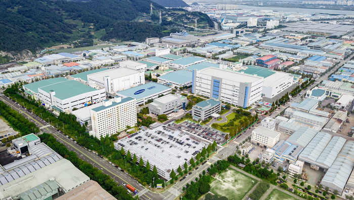
South Korea’s Samsung Electro-Mechanics will spend more on increasing its semiconductor package substrate production capacity in order to meet rising demand amid the growing high-performance semiconductor industry.
Samsung said on Monday that it decided to invest 300 billion won ($245.3 million) in the expansion of a high-performance semiconductor substrate flip chip-ball grid array (FCBGA) plant and construction of production facilities at its production complex in Busan, South Korea’s second-largest city. That will raise its total investment in package substrate production facilities to 1.6 trillion won as it was already set to spend 1.3 trillion won on its Vietnamese manufacturing subsidiary.
“With the advancement of semiconductors and the expansion of AI, cloud, and the metaverse, it is becoming crucial for semiconductor manufacturers to secure package substrate partners with technical capabilities," said Chang Duckhyun, CEO of the world’s top maker of semiconductor package substrates for flagship mobile application processors.
“We will enhance our competitiveness by focusing on the development of technologies that can provide new experiences to customers," Chang said in a statement.
HIGH-END MARKET TO GROW 20% A YEAR
The package substrate is a semiconductor package substrate that transmits electrical signals and power by connecting the high-density semiconductor chip and the mainboard. It is mainly used for central processing units (CPUs) and graphics processing units (GPUs) that require high-performance and high-density circuit connections.
The semiconductor industry requires substrate technology that can meet the increasing performance of semiconductors for servers and PCs due to the surge in demand for digital technology.
The high-end package substrate market is forecast to grow at an annual rate of 20% in the mid-to-long term as demand for various applications requiring high-speed signal processing increases, Samsung said.
Furthermore, the improvement in CPU performance has led to an increase in the number of substrate layers and demand for large-sized products. As a result, package substrates are expected to be in short supply until 2026 despite the industry’s effort to expand production, according to Samsung.
Write to Sin-Young Park at nyusos@hankyung.com
Jongwoo Cheon edited this article.
More to Read
-
 Corporate strategySamsung Electro-Mechanics to focus on IT, automotive electronics sectors
Mar 10, 2022 (Gmt+09:00)
1 Min read -
 Korean chipmakersLG Innotek, Samsung Electro-Mechanics benefit from wafer shortage
Sep 06, 2021 (Gmt+09:00)
3 Min read
Comment 0
LOG IN