ESG
Samsung Elec steps up efforts for river management
By Jan 05, 2021 (Gmt+09:00)
2
Min read
Most Read
Samsung steps up AR race with advanced microdisplay for smart glasses


When in S. Korea, it’s a ritual: Foreigners make stops at CU, GS25, 7-Eleven
Seoul-backed K-beauty brands set to make global mark
Maybe Happy Ending: A robot love story that rewrote Broadway playbook
NPS yet to schedule external manager selection; PE firms’ fundraising woes deepen


In 2019, Samsung Electronics hired a wastewater treatment expert as it ramped up efforts to recycle industrial water used at its semiconductor production lines.
Koo Tae-wan, who majored in biological wastewater treatment at POSTECH, a top technology university in Korea, is now in charge of the whole wastewater treatment process at Samsung's plants. He is credited with helping the tech giant’s Hwaseong plant earn the Carbon Trust’s Water Footprint label last September.
The Carbon Trust, an independent entity, measures and certifies the environmental footprint of organizations and products to promote low-carbon technologies and solutions.
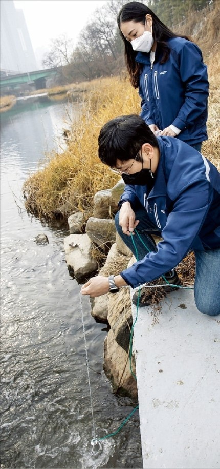
“Once a city is built, rainwater cannot permeate into the soil and nearby streams dry up. After we began to release purified wastewater into the Osan stream, which did not have enough water, the stream returned to its previous condition,” said Koo.
Samsung’s semiconductor plant in Giheung, one of its two main manufacturing facilities, discharges wastewater of up to 45,000 tons per day into the Osan stream. Since 2007, the company has been purifying the used industrial water before discharging it into the stream.
In 2019, it recycled 51% of the wastewater, up from 46% a year before. Accordingly, the water quality in the Osan stream has improved.
The industrial water used at Samsung's semiconductor production lines is classified into six categories according to its internal standards before the purification works.
Samsung’s wastewater treatment undergoes three processes: adding chemicals to remove chemical contaminants from wastewater; using small organisms to remove organic matter to comply with the required level of nitrogen concentration; and using carbon to get the remaining contaminants such as color and smell to adhere to the surface of a carbon filter.
Adding to the heavy water consumption, ultrapure water is required for the chip fabrication processes from wafter cleaning, rinsing and surface conditioning to surface cleaning, wet etch and solvent processing.
Still, South Korea does not have sufficient water supply, given its high population density and small territory compared to other countries, alongside rainfalls concentrated in summer.
“I’m writing a research paper on using the reaction of small organisms to purify chemicals used in the treatment process. Once the paper is completed, I will file a patent application,” Koo said.
Other production lines of Samsung Electronics have joined in the 3R efforts – reduce, reuse and recycle – to raise their manufacturing efficiency and thereby reduce water consumption. Such efforts are reflected in their annual evaluations.
Write to Su-bin Lee at lsb@hankyung.com
Yeonhee Kim edited this article.
More to Read
-

-

-
 ElectronicsNow, slim is in – and Samsung aims to be No. 1 with Galaxy S25 Edge
May 09, 2025 (Gmt+09:00)
-

-
 Electric vehiclesBYD’s Atto 3 overtakes Tesla’s Model Y as best-selling EV in South Korea
May 09, 2025 (Gmt+09:00)
Comment 0
LOG IN