Foundry expansion
Samsung Electronics buys land in Austin, eyes foundry expansion
By Dec 09, 2020 (Gmt+09:00)
2
Min read
Most Read
Samsung shifts to emergency mode with 6-day work week for executives


Alibaba eyes 1st investment in Korean e-commerce platform
Blackstone signs over $1 bn deal with MBK for 1st exit in Korea
NPS loses $1.2 bn in local stocks in Q1 on weak battery shares
MBK eyes stake in Korean software developer Tmaxsoft


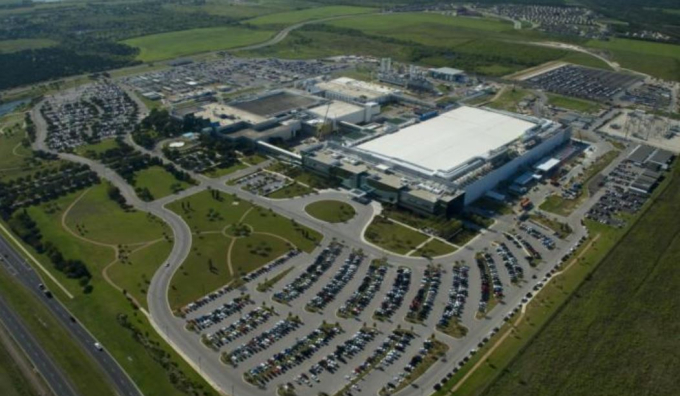
Samsung Electronics Co. has purchased a giant lot of land in Austin, Texas, where its US chip plant is located, raising expectations that the company may expand its foundry business.
According to the semiconductor industry on Dec. 8, Samsung has steadily bought a total of 104,089 square meters of land since 2018 near its Austin chip foundry plant. The size of the newly purchased land is equal to 140 soccer fields combined.
It was not known how much Samsung Austin paid for the plot. Samsung is said to be seeking approval from the Austin City Council on its plan to rezone the underdeveloped land.
A Samsung official said its zoning application is part of its strategy ŌĆ£to remain flexible in making business decisions.ŌĆØ He added that nothing yet has been decided on how to use the newly purchased land.
SPACE TO GROW IN THE US
Industry watchers, however, said Samsung is expected to expand its contract-manufacturing operations in the US by adding new foundry facilities in Austin particularly after its bigger rival Taiwan Semiconductor Manufacturing Co. (TSMC) unveiled its expansion plans.
TSMC, the worldŌĆÖs largest maker of chips for other companies, said in May it will spend $12 billion building a foundry plant with 5-nanometer technology in Arizona by 2024.
If the Taiwanese company takes more orders from US companies such as Apple Inc. and Advanced Micro Devices Inc. (AMD) after completion of its new plant, Samsung may lose some of its clients, according to industry analysts.
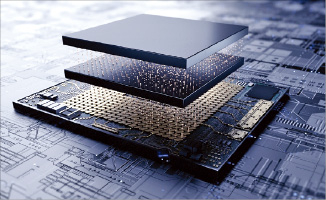
SamsungŌĆÖs Austin plant currently makes 14 nm, 28 nm and 32 nm products for other companies. More advanced 7 nm products based on its extreme ultraviolet (EUV) lithography technology are manufactured at its Pyeongtaek plant in Korea.
Samsung is the worldŌĆÖs second-largest foundry player with a market share of 16.4% in the third quarter, following industry leader TSMCŌĆÖs 53.9%, according to market tracker TrendForce.
SAMSUNG CLOSES IN ON BIGGER RIVAL TSMC
As part of its efforts to gain ground in the global chipmaking sector, Samsung last week announced a leadership change in its two key businesses ŌĆō memory chips and foundry.
Under the reshuffle, the company named Choi Si-young to take charge of its foundry business. He previously served as head of SamsungŌĆÖs memory manufacturing technology sector.
Analysts said SamsungŌĆÖs new foundry chief Choi will be asked to further narrow the gap with TSMC in coming years.
Samsung is known to be spending 10 trillion won ($8.6 billion) a year to develop chip foundry technology and purchase related equipment to close in on its bigger rival TSMC.
Currently, Samsung operates seven foundry production lines in Korea and the US.
Write to Jeong-Soo Hwang at hjs@hankyung.com
In-Soo Nam edited this article.
More to Read
-

-
 Aerospace & DefenseHanwha Aerospace, Poland sign $1.6 billion Chunmoo rocket launcher deal
51 MINUTES AGO
-
-

-
Comment 0
LOG IN