Chip packaging
Samsung foundry ramps up chip packaging to compete against TSMC
By Nov 30, 2020 (Gmt+09:00)
2
Min read
Most Read


The battleground for global foundry leaders ŌĆō Samsung Electronics Co. and Taiwan Semiconductor Manufacturing Co. (TSMC) ŌĆō is shifting from ultra-fine processing to packaging as the industry expands its turf from consignment production to comprehensive services.
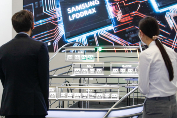
Samsung Electronics' foundry division plans to offer four types of chip packaging based on performance and price to provide a wider range of choices for its clients by the end of next year, according to the semiconductor industry on Nov. 29.┬Ā
Currently, Samsung ElectronicsŌĆÖ core packaging is X-Cube, a 3D chip stacking technology that stacks front-end processor wafers on top of each other. Also, the company has completed the 2.5D redistribution layer (RDL) service that arranges two high bandwidth memory (HBM) chips next to the logic chip.
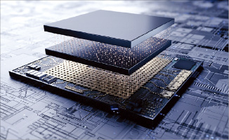
Next year, the domestic semiconductor giant plans to roll out I-Cube 8X technology that places eight HBMs aside the logic area, as well as X/I Cube technology that combines the benefits of X-Cube and I-Cube.
CHIP PACKAGING TO BOOST SAMSUNG'S COMPETITIVE EDGE
Samsung Electronics aims to be at the forefront of the packaging industry to gain a fresh edge against TSMC, which has been its competitor in the ultra-fine processing segment.
Currently, Samsung Electronics and TSMC are the only two companies in the world that offer a process below 7 nanometers (nm).
Packaging technology can help enhance semiconductor performance without having to shrink the nanometer through ultra-fine processing ŌĆōwhich is technologically challenging and requires more time.
For example, Samsung ElectronicsŌĆÖ X-Cube stacks the storage device on top of the logic, maximizing the storage space per unit area compared to the previous technology.
Samsung Electronics has selected the worldŌĆÖs No.2 semiconductor packaging company Amkor Technology Inc. as its foundry partner to broaden its packaging services.
COMPETITION HEATS UP BETWEEN SAMSUNG AND TSMC
Meanwhile, competition among foundry companies is likely to heat up as chip packaging becomes more prominent in the industry. According to French market research firm Yole Development, the semiconductor packaging market is expected to grow from $29 billion in 2019 to $42 billion in 2025.
Already foundry businesses are evolving to offer comprehensive services including both front-end and back-end processes such as electronic design automation (EDA), intellectual property (IP), design, packaging and more.
Samsung ElectronicsŌĆÖ competitor TSMC has been ramping up its chip packaging as well. In a recent board meeting, the company's proposal to invest $14.1 billion in front-end and back-end processes was approved.
Industry sources say that TSMC is currently testing its 3D SolC packaging technology similar to SamsungŌĆÖs X-Cube.
The company may produce 3D technology-based semiconductors with its major clients Google and AMD as early as 2022, according to the Japanese media outlet Nikkei.┬Ā
ŌĆ£We expect Samsung Electronics and TSMC to be locked in fierce competition over packaging technology for some time,ŌĆØ said a semiconductor industry source.
Write to Jung-soo Hwang at hjs@hankyung.com
Danbee Lee edited this article.
More to Read

Comment 0
LOG IN