Korean chipmakers
Samsung to unveil 3D DRAM in 2025 to lead AI chip market
The 3D DRAM market is likely to grow to $100 billion by 2030 as it sharply raises a chip's capacity per unit area
By Apr 02, 2024 (Gmt+09:00)
3
Min read
Most Read
Alibaba eyes 1st investment in Korean e-commerce platform


Blackstone signs over $1 bn deal with MBK for 1st exit in Korea
Korea's Lotte Insurance put on market for around $1.5 bn
OCI to invest up to $1.5 bn in MalaysiaŌĆÖs polysilicon plant
NPS loses $1.2 bn in local stocks in Q1 on weak battery shares


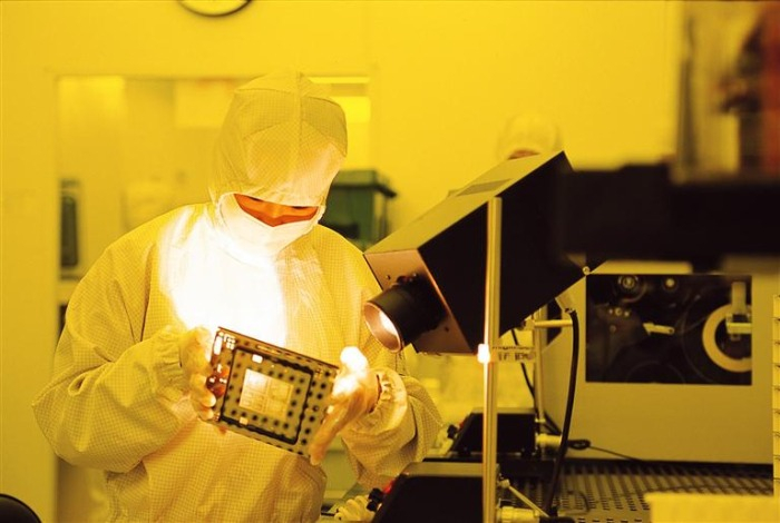
Samsung Electronics Co., the worldŌĆÖs top memory chipmaker, aims to introduce three-dimensional (3D) DRAM, a game-changer in the artificial intelligence industry, in 2025 to lead the global AI semiconductor market currently dominated by its smaller rival SK Hynix Inc.
A 3D DRAM chip triples the capacity per unit area by stacking cells vertically rather than placing them horizontally as is currently done. That compares with high bandwidth memory (HBM) that vertically interconnects multiple DRAM chips.
Samsung unveiled its 3D DRAM development roadmap at Memcon 2024, a gathering of global chipmakers, held in San Jose, California last month, according to semiconductor industry sources in Seoul on Tuesday.
The Suwon, South Korea-based tech giant plans to launch an early version of 3D DRAM in 2025 based on its vertical channel transistor technology, which vertically sets a channel, a passage for electron flow, in a transistor constituting a cell and wraps it with a gate acting as a switch.
The company also plans to introduce stacked DRAM, which piles up all cells including a capacitor, in 2030.
MARKET TO GROW TO $100 BILLION
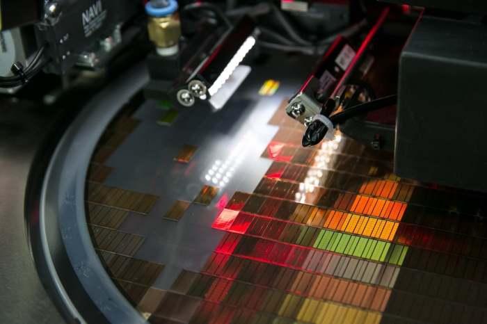
DRAM currently consists of up to 62 billion cells on a substrate with transistors densely integrated on a flat plane, making it difficult to avoid current leakage and interference.
As the transistors in 3D DRAM are stacked into multiple layers, a 3D DRAM structure is expected to widen the gaps between transistors, reducing such leakage and interference.
3D DRAM is predicted to increase capacities within a unit chip area as more cells can be put in the same area. The basic capacity of 3D DRAM is 100 gigabytes (GB), nearly triple the 36 GB maximum capacity of the currently available DRAM.
The global 3D DRAM market is likely to grow to $100 billion by 2030, industry sources said, although industry trackers have yet to make forecasts as the market is in its infancy.
LEADER OF THE AI SEMICONDUCTOR MARKET
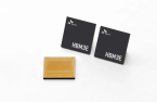
The technology is expected to help Samsung take the throne in the worldŌĆÖs AI semiconductor industry, beating SK Hynix, which currently dominates the AI chip sector with a 90% share in the global market of HBM, DRAM for AI applications, industry sources said.
Although they have been working on the technology, SamsungŌĆÖs rivals including SK Hynix and Micron Technology Inc. have yet to unveil any roadmaps for 3D DRAM.
SK Hynix has introduced its concept for 3D DRAM at various industry conferences. Micron, which started developing 3D DRAM in 2019, reportedly has about 30 patents on the technology, the most among the three chipmakers.
Chinese memory chip manufacturers accelerated the development of 3D DRAM as they saw the emerging technology as an opportunity to beat larger competitors. ChangXin Memory Technologies (CXMT), ChinaŌĆÖs top memory chipmaker, and the Chinese Academy of Sciences released their research results on 3D DRAM.
MORE CAPACITY ON SMALLER CHIP
The global DRAM industry has been developing smaller chips with more data processing capacity for more than a decade as electronic devices equipped with DRAM such as smartphones became smaller with more functions. The rapid growth of AI, which requires the quick processing of large amounts of data, is intensifying the trend.
3D DRAM is expected to meet the demand for such chips as it is smaller than the existing DRAM with higher capacity.
In the near term, the new semiconductors are likely to be used for small information technology devices such as smartphones and laptops, which require high-performance DRAM for their on-device AI functions.
The auto industry is expected to use 3D DRAM in the longer term as electric vehicles and self-driving cars need DRAM that can process large data collected from roads in real time.
TO NARROW CRITICAL DIMENSIONS
Samsung is developing technology to dominate the 3D DRAM sector to narrow its critical dimensions to 8-9 nanometers (nm) by 2027-2028. The latest DRAM is estimated to be around 12 nm.
The company is also actively expanding its workforce for 3D DRAM research and development. It opened a next-generation process development team at its semiconductor research center for the technology.
Song Jaihyuk, the corporate president and chief technology officer of SamsungŌĆÖs semiconductor business, is leading the team.
Samsung last year appointed Lee Siwoo, a 3D DRAM expert at Micron, as an executive vice president.
Write to Jeong-Soo Hwang, Chae-Yon Kim and Eui-Myung Park at hjs@hankyung.com
┬Ā
Jongwoo Cheon edited this article.
More to Read
-
 Korean chipmakersSamsung set to triple HBM output in 2024 to lead AI chip era
Mar 27, 2024 (Gmt+09:00)
3 Min read -
 Korean chipmakersSamsung to unveil Mach-1 AI chip to upend SK HynixŌĆÖs HBM leadership
Mar 20, 2024 (Gmt+09:00)
3 Min read -
 Korean chipmakersSK Hynix mass-produces HBM3E chip to supply Nvidia
Mar 19, 2024 (Gmt+09:00)
3 Min read -
 ElectronicsSamsung Galaxy S24 heralds dawning of AI smartphone era
Jan 18, 2024 (Gmt+09:00)
3 Min read -
 Korean chipmakersSamsung to unveil 3D AI chip packaging tech SAINT to rival TSMC
Nov 12, 2023 (Gmt+09:00)
3 Min read
Comment 0
LOG IN