Korean chipmakers
Samsung leader eyes memory chip packaging investment
TSMC is fast-forwarding the technology R&D as Google and Apple increase chipmaking, intensifying global competition
By Feb 17, 2023 (Gmt+09:00)
2
Min read
Most Read
LG Chem to sell water filter business to Glenwood PE for $692 million


Kyobo Life poised to buy Japan’s SBI Group-owned savings bank
KT&G eyes overseas M&A after rejecting activist fund's offer
StockX in merger talks with Naver’s online reseller Kream
Mirae Asset to be named Korea Post’s core real estate fund operator


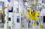
Samsung Electronics Co., the world’s largest memory chipmaker, may accelerate investment in leading-edge technologies including chip packaging, which prevents physical damage and corrosion to semiconductor materials.
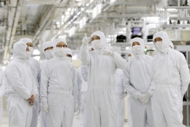
The world’s largest memory chipmaker should stick to its plan for investment and training talent, Samsung Group leader Jay Y. Lee said on Feb. 17 during his visit to packaging business sites in both Cheonan and Onyang, South Chungcheong Province in Korea.
His visit to the manufacturing sites comes 10 days after his trip to Samsung Display Asan Campus, the display unit’s main plant in Asan in the same province.
At the time, Lee highlighted that the firm should make its best efforts for both unrivaled innovation and competitiveness, showing his will to further widen the technology gap between Samsung and its global peers.
Touring the plants on Friday, the executive chairman of Samsung Electronics reviewed mid-to-long-term strategies of the chipmaking business, including the next-generation technology of semiconductor packaging and the research and development of it.
He also requested proactive investments in talent and future technology from Samsung’s key executives, including Kyung Kye-hyun, head of the semiconductor business, Choi Si-young, head of the foundry business, and Park Yong-in, the president of system large-scale integration (LSI) business division.
KEY TECHNOLOGY AT FINAL PROCESSING STAGE
Memory chip packaging is the final stage of semiconductor device fabrication to protect chip materials and connect the chips to a circuit board. Advanced packaging technology has become more important as global tech giants, such as Google LLC and Apple Inc., boost the production of their chips.
Samsung is set to make aggressive investments in chip packaging, market watchers said. It set up a team dedicated to advanced packaging businesses at the end of last year to ramp up the growth of the technology.
TSMC outperforms Samsung in chip packaging technology. The Taiwanese semiconductor giant built an integrated circuit R&D center in Tsukuba, Japan last July for silicon stacking and advanced packaging.
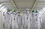
Lee is speeding up his visits to semiconductor manufacturing sites – he has toured seven plants across Korea since his inauguration as Samsung Electronics’ chairman last October.
The group’s investment in regional factories boosts not only the local economy but also the businesses of Samsung’s partner companies, a source said.
Write to Ji-Eun Jeong at jeong@hankyung.com
Jihyun Kim edited this article.
More to Read
-
 Corporate strategySamsung’s TV business launches customer marketing team
Feb 16, 2023 (Gmt+09:00)
1 Min read -
 Korean chipmakersSamsung secures $16 bn loan from display unit for chipmaking
Feb 14, 2023 (Gmt+09:00)
2 Min read -
 Korean chipmakersSamsung, SK Hynix: key beneficiaries of ChatGPT fever
Feb 13, 2023 (Gmt+09:00)
4 Min read -
 Tech, Media & TelecomSamsung to supply advanced 5G network equipment to KDDI
Feb 09, 2023 (Gmt+09:00)
3 Min read -
 Leadership & ManagementSamsung’s Lee may ramp up investment in QD-OLED panels
Feb 07, 2023 (Gmt+09:00)
2 Min read
Comment 0
LOG IN