Samsung Elec. celebrates world's first shipment of 3-nanometer chips
The 3 nm process node boasts higher performance, better area reduction and lower power usage than TSMC's 4 nm
By Jul 25, 2022 (Gmt+09:00)
LG Chem to sell water filter business to Glenwood PE for $692 million


KT&G eyes overseas M&A after rejecting activist fund's offer
Kyobo Life poised to buy Japan’s SBI Group-owned savings bank
StockX in merger talks with Naver’s online reseller Kream
Meritz backs half of ex-manager’s $210 mn hedge fund


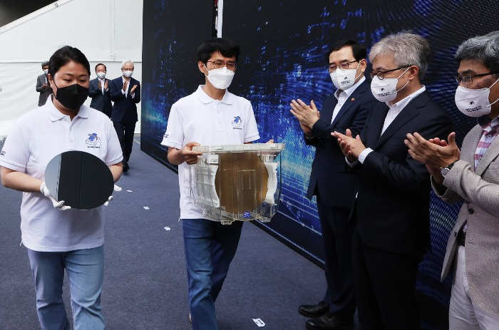
Samsung Electronics Co. held a ceremony on Monday to celebrate its first shipment of 3-nanometer semiconductor chips, notching its lead in the race to manufacture the most advanced chips on the market.
The electronics giant held the event at its Hwaseong production center, about 40 kilometers south of the capital Seoul.
Samsung announced that its first-generation 3 nm process node achieves 23% higher performance, 16% area reduction, and 45% less power consumption than previous chips.
Samsung has brought the advanced chipmaking technology to market ahead of foundry rival Taiwan Semiconductor Manufacturing Company (TSMC).
"Samsung has opened a new chapter in the foundry business with the launch of mass production of 3 nm chips. The earlier-than-expected development of gate-all-around (GAA) technology, as an alternative to the FinFET process, was a breakthrough in innovation,” said Kyung Kye-hyun, CEO of the company's device solutions division.
MASS PRODUCTION
On June 30, Samsung announced it had begun mass production of the 3 nm chips for the first time in the world.
Two years prior, the world’s largest foundry TSMC confirmed it is planning to crank out chips based on a 4 nm manufacturing process and has been mass producing them since.
Industry insiders say the development of 3 nm chips allows Samsung to outperform its Taiwanese rivals.
In semiconductor manufacturing, the 3 nm process has been the next die shrink following the 5 nm MOSFET technology node. TSMC had plans to produce 3 nm chips by the second half of this year.
Samsung's 3 nm process is based on gate-all-around field-effect transistor (GAAFET) technology, a type of multi-gate MOSFET technology, whereas TSMC's 3 nm process will still use fin field-effect transistor (FinFET) technology.
According to market research firm OMNIA, the Taiwanese company had a whopping 49.5% market share of the global foundry industry. The figure is more than three times Samsung Electronics' share, which stands at 16.3%.

GAA TECH
Experts say the technological difference would be advantageous for Samsung, even after TSMC develops its own 3 nm.
Samsung is confident the next-generation 3 nm chips built on GAA technology will eventually allow 25% better performance than the existing FinFET process.
When it comes to chips, smaller nanometers means faster processing.
In chips with small nanometers, transistors are packed tightly and the distance between each transistor is small. Since the electrons need to travel a shorter distance, the electrical signal passes through faster, resulting in faster processing.
The race to reduce nanometers has slowed in recent years due to the increasing difficulty of doing so.
Semiconductors work on the back of an imbalance of electrons that carry a negative charge.
The imbalance generates positive and negative charges at two ends of the semiconductor material. The smaller the nanometer, the smaller its control system has to be, which leaves room for leakage of current.
To keep the chances of current leakage affecting chip performance at a minimum, Samsung applied FinFET technology for the manufacture of 5-nm semiconductors.
However, the GAA technology used in building 3 nm chips leaves even less room for current leakage.
The second-generation 3 nm process node based on GAA technology, forecast to be complete next year, will have 30% higher performance, 35% area reduction, and 50% lower power consumption than a FinFET-based 5 nm node.
Write to Sin-Young Park at nyusos@hankyung.com
Jee Abbey Lee edited this article.
-
 Korean chipmakersSamsung Elec's Q2 earnings signal end of upward run
Jul 07, 2022 (Gmt+09:00)
3 Min read -
 Supply chainS.Korean trucker strike enters 3rd day, targets Samsung’s supply chain
Jun 09, 2022 (Gmt+09:00)
3 Min read