Yoon, Biden highlight 'economic security alliance' following Samsung tour
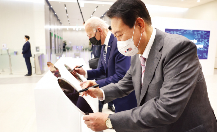
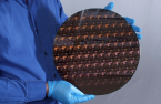
The two leaders signed wafers like a guest book after a guided tour by the conglomerate's de facto leader Jay Y. Lee
By May 20, 2022 (Gmt+09:00)
LG Chem to sell water filter business to Glenwood PE for $692 million


Kyobo Life poised to buy Japan’s SBI Group-owned savings bank
KT&G eyes overseas M&A after rejecting activist fund's offer
StockX in merger talks with Naver’s online reseller Kream
Mirae Asset to be named Korea Post’s core real estate fund operator


South Korean President Yoon Suk-yeol and visiting US President Joe Biden emphasized the two countries' iron-clad commitment to economic security alliance on Friday.
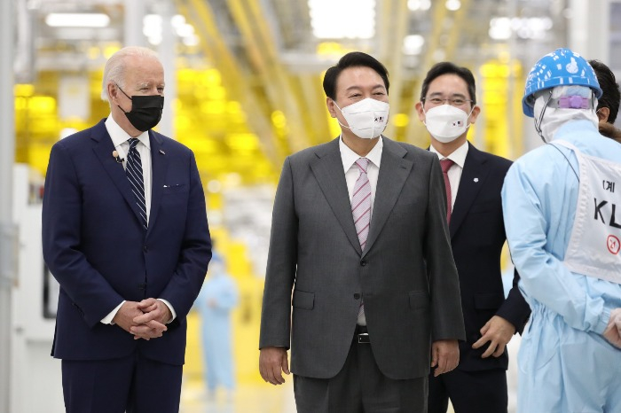
Biden began his three-day visit to the peninsula with a tour of Samsung Electronics Co.'s complex in Pyeongtaek, the world’s largest semiconductor plant.
The 79-year-old arrived at the US Osan Air Base early afternoon and immediately headed to the chipmaking facility located some 70 kilometers south of Seoul.
Once there, he was joined by the newly elected Yoon.
Vice Chairman of Samsung Electronics Jay Y. Lee greeted the two heads of state and showed them around the highly guarded facility.
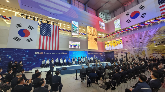
“Following today’s visit, I hope for a renewed Korea-US alliance that encompasses cutting-edge technology and the related supply network,” Yoon said during a joint address after the tour.
Biden described the start of his Asia tour with a visit to the Samsung semiconductor facility to be “emblematic of the future of cooperation and innovation that our nations can and must build together."
Biden described the 3-nanometer semiconductor as "the key to propelling us into the next era of humanity’s technological development: artificial intelligence, quantum technologies, 5G, and so very much more — things we haven’t even thought of at this point."
The two heads of state used the semiconductor wafers as a guest book after the tour.
Semiconductor plants are heavily guarded as the layout and related details are considered commercial confidentiality. Experts say opening up the facility to a foreign head of state and his entourage was an unprecented show of confidence in the Korea-US alliance.
The US commander in chief also touted Samsung's investment into the United States.
A year ago, Samsung Electronics announced its plan to pour in $17 billion into building a semiconductor fab in Taylor, Texas. The facility is poised to be operational in the second half of 2024.
Biden elaborated that the investment will create 3,000 new high-tech jobs in Texas and add to 20,000 jobs Samsung already supports in the country.
Industry insiders are hopeful the strengthened Seoul-Washington semiconductor industry alliance would reshape the US-led supply network and cap China’s rising prowess in the semiconductor sector.
FOUNDRY RELIANCE
But American car manufacturers like General Motors Co. and Ford Motor Co. have been battling semiconductor shortages, especially during the pandemic.
Global technology behemoths such as Google, Amazon, and Meta are not only racing to secure enough semiconductors to build servers but to find foundries that can manufacture chips designed by them.
Samsung Electronics takes a 43.5% share of the DRAM chip market worldwide. When combined with SK Hynix Inc., the two firms account for a whopping 70% of the world’s DRAM chip market.
The South Korean chipmaker's share in the global foundry market rose 1.1 percentage points to reach 18.3% in the October-December period last year, according to market analyst firm TrendForce. Taiwan's TSMC slid slightly but maintains the No. 1 spot with a 52.1% market share.
Apple and Qualcomm are clients of both the Samsung Electronics and TSMC foundries. In fact, Qualcomm CEO Cristiano Amon was seen beside Biden during his Pyeongtaek visit Friday.
Some industry insiders say the strengthened alliance between Washington and its allies such as Seoul and Taipei could put a cap on China’s growing semiconductor industry.
For example, Chinese fabless semiconductor company HiSilicon cannot fully operate without a foundry that works with it. HiSilicon is wholly owned by Huawei.
Others say that Biden’s visit to the Pyeongtaek plant highlights the South Korean electronics giant's importance to the US economy.
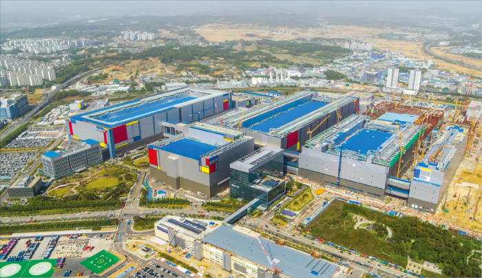
The Pyeongtaek campus is Samsung's key facility for next-generation chips. The world’s largest semiconductor plant spans 2.89 million square meters, equivalent to the size of 400 soccer fields combined.
$170 BILLION TARGET
The Yoon administration earlier revealed its mid- to long-term roadmap on how to assist the domestic semiconductor industry.
Prior to the presidential transition, the committee tasked with the change announced the plan on May 3. In it, the team vowed to bring South Korea’s cutting-edge technology sectors such as the semiconductor, battery, and artificial intelligence industries to not only an unmatched, but an “unprecedented level.”
The new administration plans to provide hefty incentives for investments into semiconductor facilities and expedite the approval process for such construction.
The transition committee had said it will also encourage the opening of special universities for the semiconductor industry and a higher number of accepted students into the existing ones.
The Yoon administration plans to bump up South Korea’s semiconductor exports by 30% to reach $170 billion by 2027.
3-NM CHIP
In addition to the facility’s massive size, Jay Y. Lee showcased the next-generation 3-nanometer semiconductor built on the Gate-All-Around (GAA) technology to the two leaders.
The South Korean conglomerate is slated to mass produce the new product within the next couple of months.
As the only son of former Samsung chairman Lee Kun-hee, Jay Y. Lee is the de facto leader of the group despite officially serving as its vice chairman for now.
"Lee could present a 3-nm chip to Biden to emphasize the company's prowess over Taiwan's TSMC in the sector," an industry insider with the knowledge of the latest technology told The Korea Economic Daily prior to the tour.
The GAA process minimizes the size of a chip by up to 35% while providing 30% higher performance, or 50% lower power consumption – compared to the 5-nm process, according to Samsung.
The world's largest contract chip manufacturer TSMC and Samsung have been in cut-throat competition to outperform each other by mass producing the 3-nm chips.
Write to In Yeop Kim, Sin-Young Park, Jee Abbey Lee at inside@hankyung.com
Jee Abbey Lee edited this article.
-
 Business & PoliticsTrump Jr. meets Korean business chiefs in back-to-back sessions
Apr 30, 2025 (Gmt+09:00)
-
 Korean chipmakersSamsung in talks to supply customized HBM4 to Nvidia, Broadcom, Google
Apr 30, 2025 (Gmt+09:00)
-
 EnergyLS Cable breaks ground on $681 mn underwater cable plant in Chesapeake
Apr 29, 2025 (Gmt+09:00)
-
 Business & PoliticsUS tariffs add risk premium to dollar assets: Maurice Obstfeld
Apr 29, 2025 (Gmt+09:00)
-